Datasheet Summary
Standard LCD Segment Driver
BU9796Axxx Series MAX 80 segments (SEG20×4)
- Features
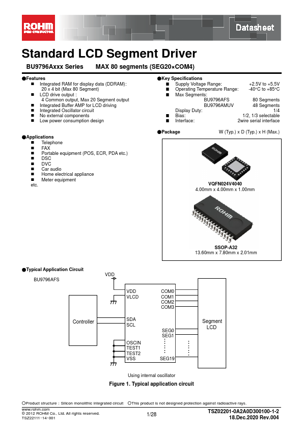
- Integrated RAM for display data (DDRAM): 20 x 4 bit (Max 80 Segment)
- LCD drive output : 4 mon output, Max 20 Segment output
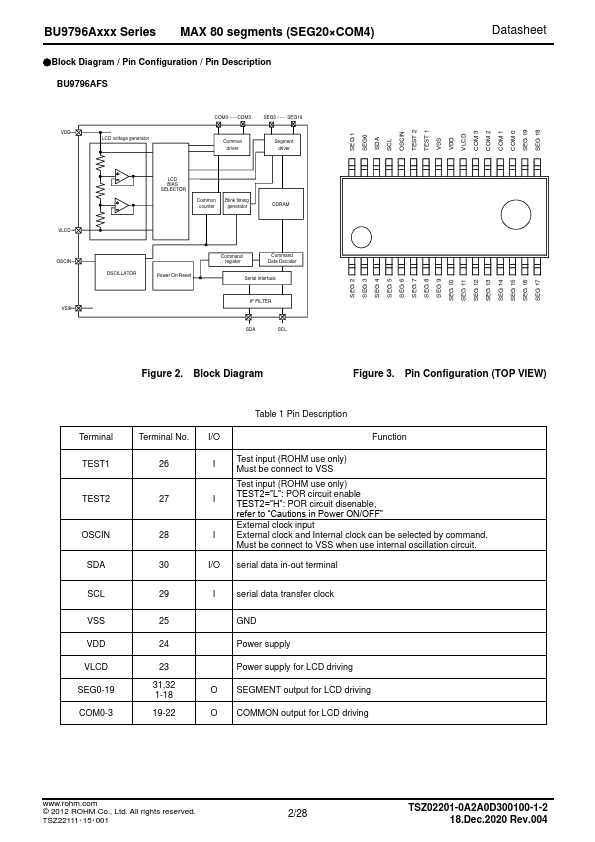
- Integrated Buffer AMP for LCD driving
- Integrated Oscillator circuit
- No external ponents
- Low power consumption design
- Applications
- Telephone
- FAX
- Portable equipment (POS, ECR, PDA etc.)
- DSC
- DVC
- Car audio
- Home electrical appliance
- Meter equipment etc.
- Key Specifications
- Supply Voltage Range:
+2.5V to +5.5V
- Operating Temperature Range: -40°C to +85°C
- Max Segments:
80 Segments
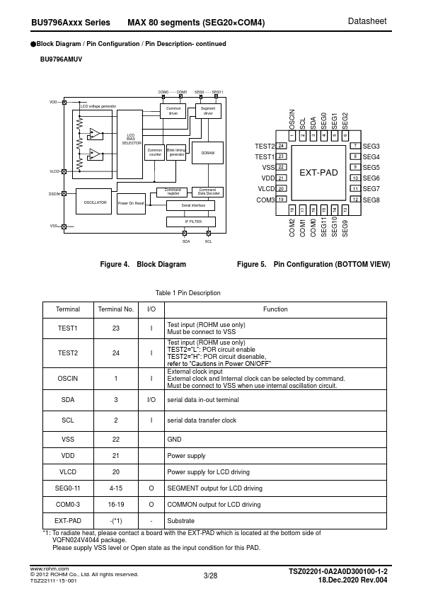
BU9796AMUV
48 Segments
Display...


