ROHM Semiconductor UMF6N
Dual Transistor
| Part No. | UMF6N |
|---|---|
| Datasheet | UMF6N Download |
| Manufacturer |  ROHM Semiconductor |
| Description | Dual Transistor |
| Buy | Stock & Price |

FEATURES
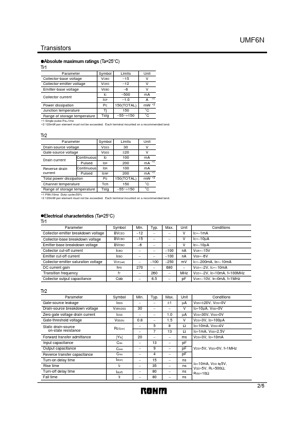
1) Power switching circuit in a single package. 2) Mounting cost and area can be cut in half. (4) 0.65 1.3 0.7 0.9 (3) 0.2 (6) 0.1Min. Each lead has same dimensions (1) 2.0 (5) (2) 1/5 UMF6N Transistors !Absolute maximum ratings (Ta=25°C) Tr1 Limits Symbol −15 VCBO −12 VCEO −6 VEBO −500 IC Collector current −1.0 ICP 150(TOTAL) PC Power dissipation Tj 150 Junction temperature Tstg −55~+150 Range of storage temperature Parameter Collector-base voltage Collector-emitter voltage Emitter-base voltage Unit V V V mA A mW °C °C ∗1 ∗2 ∗1 Single pulse PW=1ms ∗2 120mW per element must not be exceeded. Each terminal mounted on a recommended land. Tr2 Symbol Limits Parameter VDSS 30 Drain-source voltage VGSS ±20 Gate-source voltage ID 100 Continuous Drain current 200 IDP Pulsed IDR 100 Continuous Reverse drain current IDRP 200 Pulsed Total power dissipation 150(TOTAL) PD Tch 150 Channel temperature Tstg −55~+150 Range of storage temperature Unit V V mA mA mA mA mW °C °C ∗1 ∗1 ∗2 ∗1 PW≤10ms Duty cycle≤50% ∗2 120mW per element must not be exceeded.