K7A161830B Overview
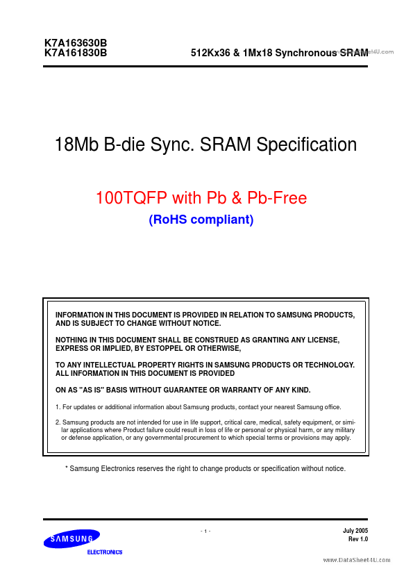
100TQFP with Pb & Pb-Free (RoHS pliant) INFORMATION IN THIS DOCUMENT IS PROVIDED IN RELATION TO SAMSUNG PRODUCTS, AND IS SUBJECT TO CHANGE WITHOUT NOTICE. NOTHING IN THIS DOCUMENT SHALL BE CONSTRUED AS GRANTING ANY LICENSE, EXPRESS OR IMPLIED, BY ESTOPPEL OR OTHERWISE, TO ANY INTELLECTUAL PROPERTY RIGHTS IN SAMSUNG PRODUCTS OR TECHNOLOGY. ALL INFORMATION IN THIS DOCUMENT IS PROVIDED ON AS "AS IS" BASIS WITHOUT GUARANTEE OR WARRANTY OF ANY KIND. • Synchronous Operation. • 2 Stage Pipelined operation with 4 Burst. • On-Chip Address Counter. • Self-Timed Write Cycle. • On-Chip Address and Control Registers. • VDD= 2.5 or 3.3V +/- 5% Power Supply. • 5V Tolerant Inputs Except I/O Pins. • Byte Writable Function. • Global Write Enable Controls a full bus-width write. • Power Down State via ZZ Signal. • LBO Pin allows a choice of either a interleaved burst or a linear burst. • Three Chip...
K7A161830B Key Features
- Synchronous Operation
- 2 Stage Pipelined operation with 4 Burst
- On-Chip Address Counter
- Self-Timed Write Cycle
- On-Chip Address and Control Registers
- VDD= 2.5 or 3.3V +/- 5% Power Supply
- 5V Tolerant Inputs Except I/O Pins
- Byte Writable Function
- Global Write Enable Controls a full bus-width write
- Power Down State via ZZ Signal
K7A161830B Applications
- Samsung Electronics reserves the right to change products or specification without notice