FKI10126
Features
- V(BR)DSS --------------------------------100 V (ID = 100 µA)
- ID ---------------------------------------------------------- 41 A
- RDS(ON) -------- 12.1 mΩ max. (VGS = 10 V, ID = 33.0 A)
- Qg------ 45.2n C (VGS = 4.5 V, VDS = 50 V, ID = 33.0 A)
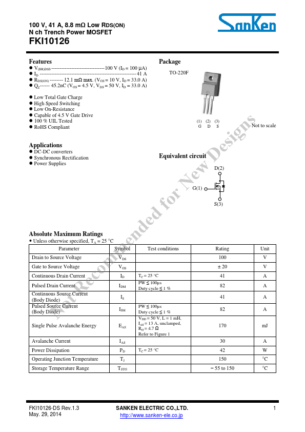
Package
TO-220F
- Low Total Gate Charge
- High Speed Switching
- Low On-Resistance
- Capable of 4.5 V Gate Drive
- 100 % UIL Tested
- Ro HS pliant
Applications
- DC-DC converters
- Synchronous Rectification
(1) (2) (3) s G D S Design Equivalent circuit
Not to scale or New
- Power Supplies
D(2) G(1)
S(3) ded f Absolute Maximum Ratings n
- Unless otherwise specified, TA = 25 °C e Parameter
Symbol m Drain to Source Voltage
VDS m Gate to Source Voltage
VGS o Continuous Drain Current
ID ec Pulsed Drain Current
R Continuous Source Current
(Body Diode)
IS t Pulsed Source Current No (Body Diode)
Test conditions
TC = 25 °C PW ≤ 100µs Duty cycle ≤ 1 %
PW ≤ 100µs Duty cycle ≤ 1 % VDD = 50 V, L = 1 m H,
Rating...