SDC9300
Key Features
- a high pulse current buffer design to maximize Minimizes the effect of output shoot-through
- The upper channel can drive up to 600V NMOS tube or IGBT
- 1.0ÿÿÿÿÿÿÿÿÿÿÿÿÿÿÿÿÿÿÿÿÿÿÿÿÿÿÿÿÿÿÿÿÿ 1/9 ©2016 Shaoxing Devechip Microelectronics Co., Ltd.ÿÿÿÿÿÿÿÿÿÿÿÿÿÿÿÿÿÿÿÿÿÿÿÿÿÿÿÿÿÿÿÿÿÿÿ .sdcÿsemi
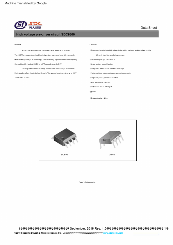
- Machine Translated by Google High voltage pre-driver circuit SDC9300 Pin Description Data Sheet serial number 1 2 3 4 5 6 7 8