SEMIWILL SW226N
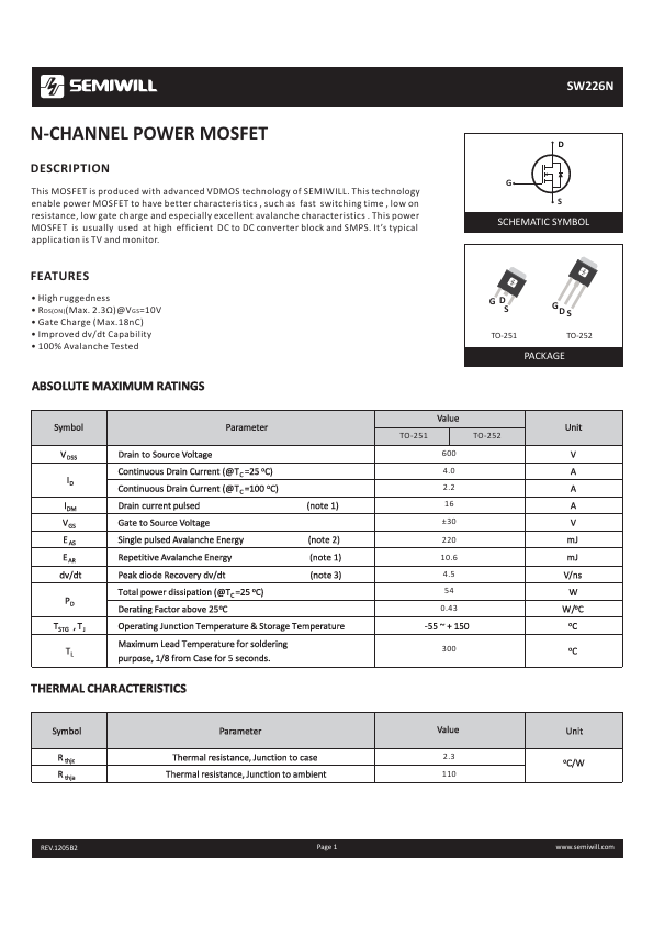
This MOSFET is produced with advanced VDMOS technology of SEMIWILL. This technology enable power MOSFET to have better characteristics , such as fast switching time , low on resistance, low gate charge and especially excellent avalanche characteristics .| Part No. | SW226N |
|---|---|
| Datasheet | SW226N Download |
| Manufacturer |  SEMIWILL |
| Description | N-Channel Power MOSFET |
| Buy | Stock & Price |
DESCRIPTION
This power MOSFET is usually used at high efficient DC to DC converter block and SMPS. It’s typical application is TV and monitor. G D S SCHEMATIC SYMBOLFEATURES
● High ruggedness● R DS(ON) (Max. 2.3 Ω)@V GS=10V
● Gate Charge (Max.18nC)
● Improved dv/dt Capability
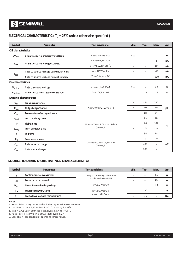
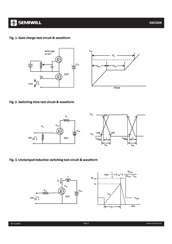
● 100% Avalanche Tested GD S TO-251 GD S TO-252 PACKAGE TO-251 600 4.0 2.2 16 ±30 220 10.6 4.5 54 0.43 TO-252 300 2.3 110 05081.R11 2/11 REV.1205B2 Page 11 SW226N PP0640SA - PP3500SC V GS =0V,I D =250uA V DS =600V,V GS =0V V DS =480V,T C =125 C V DS =30V,V GS =0V V DS =-30V,V GS =0V 600 10 V DS =V GS ,I D =250uA V GS =10V,I D =2.0A 2.0 1.9 4.0 2.3 571 V GS =0V,V DS =25V,f=1MHz 70 18 21 V DS =300V,I D =4.0A,R G =25ohm (note 4,5) 46 102 34 18 V DS =480V,V GS =10V,I D =4.0A (note 4,5) 3.0 6.0 740 90 24 52 102 214 78 28 Integral reverse p-n Junction diode in the MOSFET I S =4.0A, V GS =0V I S =4.0A, V GS =0V dI F /d t =100A/us Notes 1. Repeatitive rating : pulse width limited by junction temperature. 2. L = 25mH, I AS = 4.0A, V DD = 50V, R G =25Ω, Starting T J = 25 C 3.