DESCRIPTION
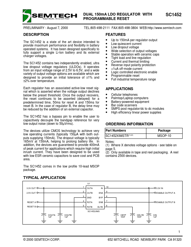
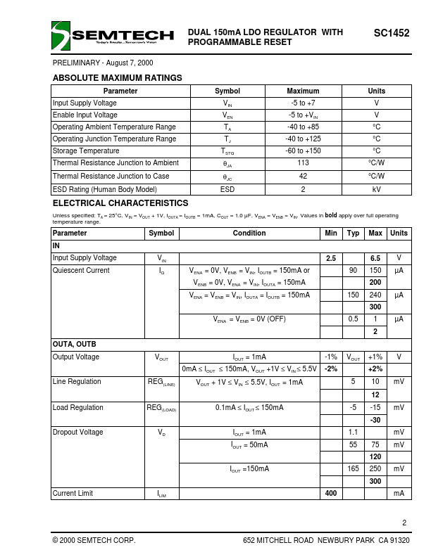
It operates from an input voltage range of 2.5V to 6.5V, and a wide variety of output voltage options are available which are designed to provide an initial tolerance of ±1% and ±2% over temperature. Each regulator has an associated active-low reset signal which is asserted when the voltage output declines below the preset threshold. Once the output recovers, the reset continues to be asserted (delayed) for a predetermined time, 50ms for reset A and 150ms for reset B. In the case of regulator B, the delay time may be reduced by the addition of an external capacitor. The SC1452 has a bypass pin to enable the user to capacitively decouple the bandgap reference for very low output noise (down to 50µVrms). The devices utilize CMOS technology to achieve very low operating currents (typically 150µA with both outputs supplying 150mA). The dropout voltage is typically 165mV at 150mA, helping to prolong battery life. In addition, the devices are guaranteed to provide 400mA of peak current for applications which require high initial inrush current. Semtech Corporation