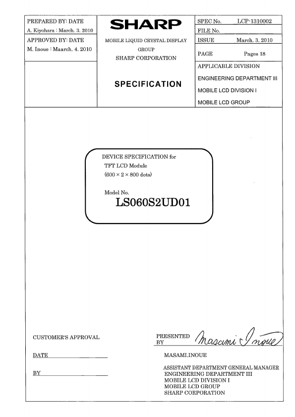
Sharp LS060S2UD01
This publication is the proprietary of SHARP and is copyrighted, with all rights reserved. The application circuit examples in this publication are provided to explain the representative applications of SHARP's devices and are not intended to guarantee any circuit design or permit any industrial property right or other rights to be executed.| Part No. | LS060S2UD01 |
|---|---|
| Datasheet | LS060S2UD01 Download |
| Manufacturer |  Sharp |
| Description | LCD Module |
| Buy | Stock & Price |
DESCRIPTION
1 GND - Ground 2 N.C.(VPP) - No Connection 3 BUSSEL I Data bas selection signal 4 RESETB I Reset signal(Active Low) 5 CSB I Chip select signal 6 RS I Display Data/Command selection signal 7 WR I Wite Enable 8 RD I Read Enable 9 D00 I/O Data bus 0 10 D01 I/O Data bus 1 11 D02 I/O 12 D03 I/O Data bus 2 Data bus 3 13 D04 I/O Data bus 4 14 D05 I/O Data bus 5 15 D06 I/O Data bus 6 16 D07 I/O Data bus 7 17 D08 I/O Data bus 8 18 D09 I/O Data bus 9 19 D10 I/O Data bus 10 20 D11 I/O Data bus 11 21 D12 I/O Data bus 12 22 D13 I/O Data bus 13 23 D14 I/O Data bus 14 24 D15 I/O Data bus 15 25 ACK O ACK signal output 26 OVSYNC O Vertical synchronizing signal output 27 N.C.(OTPTEST) - No Connection Power supply generation circuit enable 28 VDDL_EN I (Active