DESCRIPTION
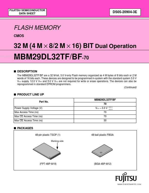
12.0 V VPP and 5.0 V VCC are not required for write or erase operations. The devices can also be reprogrammed in standard EPROM programmers. (Continued) s PRODUCT LINE UP Part No. Power Supply Voltage (V) Max Access Time (ns) Max CE Access Time (ns) Max OE Access Time (ns) MBM29DL32TF/BF 70 VCC = 3.0 V 70 70 30 +0.6 V −0.3 V s PACKAGES 48-pin plastic TSOP (1) Marking side 48-ball plastic FBGA (FPT-48P-M19) (BGA-48P-M12) MBM29DL32TF/BF-70 ) (Continued) MBM29DL32TF/BF are organized into four physical banks; Bank A, Bank B, Bank C and Bank D, which are considered to be four separate memory arrays operations. It is the Fujitsu’s standard 3.0 V only Flash memories, with the additional capability of allowing a normal non-delayed read access from a non-busy bank of the array while an embedded write (either a program or an erase) operation is simultaneously taking place on the other bank. In the device, a new design concept called FlexBankTM *1 Architecture is implemented. Using th... SPANSION