MB84VD21181EM-70 Overview
.. FUJITSU SEMICONDUCTOR DATA SHEET DS05-50307-1E Stacked MCP (Multi-Chip Package) FLASH MEMORY & SRAM 16M (×8/×16) FLASH MEMORY & 4M (×8/×16) STATIC RAM MB84VD2118XEM-70/MB84VD2119XEM-70.
MB84VD21181EM-70 Key Features
- Power Supply Voltage of 2.7 V to 3.3 V
- High Performance 70 ns maximum access time (Flash) 70 ns maximum access time (SRAM)
- Operating Temperature -40 °C to +85 °C
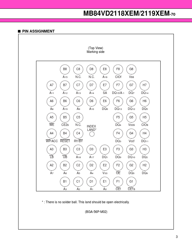
- Package 56-ball FBGA
- Both VCCf and VCCs must be in remended operation range when either part is being accessed
- FLASH MEMORY
- Simultaneous Read/Write Operations (Dual Bank) Miltiple devices available with different bank sizes (Please refer to ORD
- Minimum 100,000 Write/Erase Cycles
- Sector Erase Architecture Eight 4 K words and thirty one 32 K words. Any bination of sectors can be concurrently erased.
- Boot Code Sector Architecture MB84VD2118XEM: Top sector MB84VD2119XEM: Bottom sector