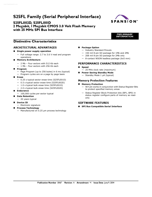
FEATURES
Memory Protection — W# pin works in conjunction with Status Register Bits to protect specified memory areas — Status Register Block Protection bits (BP1, BP0) in status register configure parts of memory as readonly SOFTWARE FEATURES
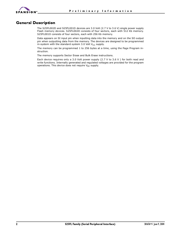
SPI Bus Compatible Serial Interface Publication Number 30167 Revision A Amendment +1 Issue Date June 9, 2004 P r e l i m i n a r y I n f o r m a t i o n GENERAL DESCRIPTION
S25FL002D consists of four sectors, each with 512 Kb memory. S25FL001D consists of four sectors, each with 256 Kb memory. Data appears on SI input pin when inputting data into the memory and on the SO output pin when outputting data from the memory. The memory can be programmed 1 to 256 bytes at a time, using the Page Program instruction. The memory supports Sector Erase and Bulk Erase instructions. Each device requires only a 3.0 Volt power supply (2.7 V to 3.6 V ) for both read and write functions. Internally generated and regulated voltages are provided for the program operations. SPANSION