SFF11N80
SFF11N80 is N-Channel Power MOSFET manufactured by SSDI.
Features
:
- -
- -
- -
- -
- -
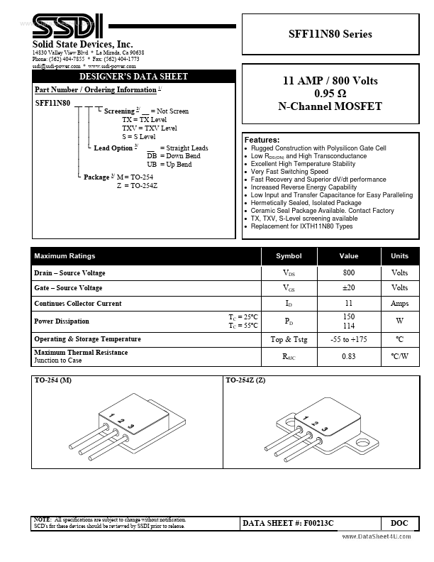
- Rugged Construction with Polysilicon Gate Cell Low RDS(ON) and High Transconductance Excellent High Temperature Stability Very Fast Switching Speed Fast Recovery and Superior d V/dt performance Increased Reverse Energy Capability Low Input and Transfer Capacitance for Easy Paralleling Hermetically Sealed, Isolated Package Ceramic Seal Package Available. Contact Factory TX, TXV, S-Level screening available Replacement for IXTH11N80 Types
DB = Down Bend UB = Up Bend Package 3/ M = TO-254 Z = TO-254Z
Maximum Ratings Drain
- Source Voltage Gate
- Source Voltage Continues Collector Current Power Dissipation Operating & Storage Temperature Maximum Thermal Resistance Junction to Case TO-254 (M) TO-254Z (Z) TC = 25ºC TC = 55ºC
Symbol
Value
Units
VDS VGS ID PD Top & Tstg RθJC
800 ±20 11 150 114 -55 to +175 0.83
Volts Volts Amps W ºC ºC/W
NOTE: All specifications are subject to change without notification. SCD's for these devices should be reviewed by SSDI prior to release.
DATA SHEET #: F00213C
..
Solid State Devices, Inc.
14830 Valley View Blvd
- La Mirada, Ca 90638 Phone: (562) 404-7855
- Fax: (562) 404-1773 ssdi@ssdi-power.
- .ssdi-power.
SFF11N80 Series
Electrical Characteristics 4/ Drain to Source Breakdown Voltage (VGS = 0V, ID = 250µA) Drain to Source On State Resistance (VGS = 10V, ID = 5.5A) On State Drain Current (VDS > ID(on) x RDS(on) Max, VGS = 10V) Gate Threshold Voltage (VDS = VGS, ID = 250µA) Gate to Source Leakage (VGS = ±20V) Zero Gate Voltage Drain Current (VGS = 0V) Forward Transconductance
- (VDS > ID(on) x RDS(on) Max, ID = 5.5A) Total Gate Charge Gate to Source Charge Gate to Drain Charge Turn on Delay Time Rise Time Turn on Delay Time Fall Time Diode Forward Voltage
- (IF = 11A, VGS = 0V) Diode Reverse Recovery Time (IF = 11A, di/dt = 100A/µsec) Input Capacitance Output Capacitance Reverse Transfer Capacitance
NOTES:
- Pulse Test: Pulse Width = 300µsec, Duty Cycle = 2% 1/ For Ordering Information,...