1803DFH
1803DFH is ST1803DFH manufactured by STMicroelectronics.
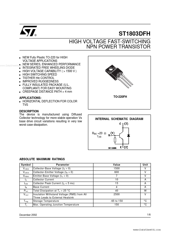
DESCRIPTION
The device is manufactured using Diffused Collector technology for more stable operation Vs base drive circuit variations resulting in very low worst case dissipation.
TO-220FH
INTERNAL SCHEMATIC DIAGRAM
RBE =20 Ω
Typ.
ABSOLUTE MAXIMUM RATINGS
Symbol V CBO V CEO V EBO IC I CM IB P tot V isol T stg Tj Parameter Collector-Base Voltage (I E = 0) Collector-Emitter Voltage (I B = 0) Emitter-Base Voltage (I C = 0) Collector Current Collector Peak Current (t p < 5 ms) Base Current Total Dissipation at T c = 25 o C Insulation Withstand Voltage (RMS) from All Three Leads to External Heatsink Storage Temperature Max. Operating Junction Temperature Value 1500 600 7 10 15 4 40 2500 -65 to 150 150 Unit V V V A A A W V o o
December 2002
1/6
ST1803DFH
THERMAL DATA
R thj-case Thermal Resistance Junction-case Max 3.125 o
C/W
ELECTRICAL CHARACTERISTICS (Tcase = 25 o C unless otherwise specified)
Symbol I CES I EBO
..
Parameter Collector Cut-off Current (V BE = 0) Emitter Cut-off Current (I C = 0) Emitter-Base Breakdown Voltage (I C = 0) Collector-Emitter Saturation Voltage Base-Emitter Saturation Voltage DC Current Gain
Test Conditions V CE = 1500 V V CE = 1500 V V EB = 4 V I E = 700 m A Tj = 125 o C
Min.
Typ.
Max. 1 2
Unit m A m A m A V
130 7
V (BR)EBO
V CE(sat) ∗ V BE(sat) ∗ h FE ∗
IC = 4 A IC = 4 A IC = 4 A IC = 1 A I C = 4.5 A I C = 4.5 A IF = 5 A IC = 4 A LB = 5 µH f = 16 KHz
I B = 0.8 A I B = 1.2 A I B = 0.8 A V CE = 5 V V CE = 1 V V CE = 5 V I Bon(END) = 0.8 A V BB = -2.5 V (see figure 1) 10 5
5 1.5 1.2
15 5 1.5 2.7 0.3
20 9 2 4 0.6 V µs µs
VF ts tf
Diode Forward Voltage INDUCTIVE LOAD Storage Time Fall Time
∗ Pulsed: Pulse duration = 300 µs, duty cycle 1.5 %
Safe Operating Area
Thermal...