1GW3B2AN6
Key Features
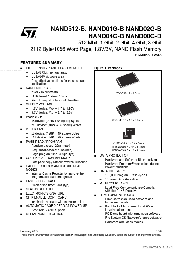
- HIGH DENSITY NAND FLASH MEMORIES - Up to 8 Gbit memory array - Up to 64Mbit spare area - Cost effective solutions for mass storage applications NAND INTERFACE - x8 or x16 bus width - Multiplexed Address/ Data - Pinout compatibility for all densities SUPPLY VOLTAGE - 1.8V device: VDD = 1.7 to 1.95V - 3.0V device: VDD = 2.7 to 3.6V PAGE SIZE - x8 device: (2048 + 64 spare) Bytes - x16 device: (1024 + 32 spare) Words BLOCK SIZE - x8 device: (128K + 4K spare) Bytes - x16 device: (64K + 2K spare) Words PAGE READ / PROGRAM - Random access: 25µs (max) - Sequential access: 50ns (min) - Page program time: 300µs (typ) COPY BACK PROGRAM MODE - Fast page copy without external buffering CACHE PROGRAM AND CACHE READ MODES - Internal Cache Register to improve the program and read throughputs FAST BLOCK ERASE - Block erase time: 2ms (typ) STATUS REGISTER ELECTRONIC SIGNATURE CHIP ENABLE ‘DON’T CARE’ - for simple interface with microcontroller AUTOMATIC PAGE 0 READ AT POWER-UP - Boot from NAND support SERIAL NUMBER OPTION Figure
- Packages