H8NB90FI
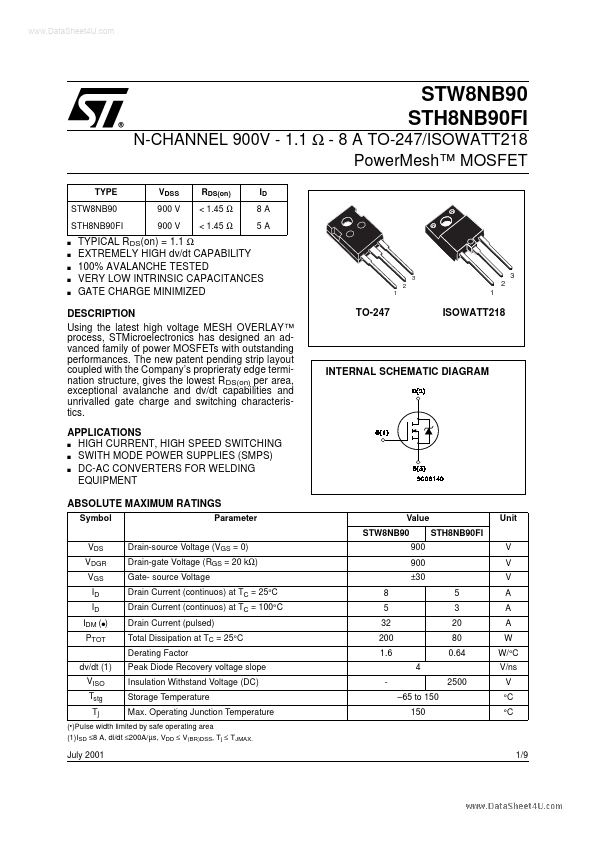
DESCRIPTION
Using the latest high voltage MESH OVERLAY ™ process, STMicroelectronics has designed an advanced family of power MOSFETs with outstanding performances. The new patent pending strip layout coupled with the pany’s proprieraty edge termination structure, gives the lowest R DS(on) per area, exceptional avalanche and dv/dt capabilities and unrivalled gate charge and switching characteristics. APPLICATIONS s HIGH CURRENT, HIGH SPEED SWITCHING s SWITH MODE POWER SUPPLIES (SMPS) s DC-AC CONVERTERS FOR WELDING EQUIPMENT ABSOLUTE MAXIMUM RATINGS
Symbol VDS VDGR VGS ID ID IDM (q) PTOT dv/dt (1) VISO Tstg Tj Parameter Drain-source Voltage (VGS = 0) Drain-gate Voltage (RGS = 20 kΩ) Gate- source Voltage Drain Current (continuos) at TC = 25°C Drain Current (continuos) at TC = 100°C Drain Current (pulsed) Total Dissipation at TC = 25°C Derating Factor Peak Diode Recovery voltage slope Insulation Withstand Voltage (DC) Storage Temperature Max. Operating Junction Temperature
ISOWATT218...