M30W0R6500T0 Overview
Key Features
- MULTI-CHIP PACKAGE – 1 die of 64 Mbit (4Mb x
- Flash Memory – 1 die of 32 Mbit (2Mb x
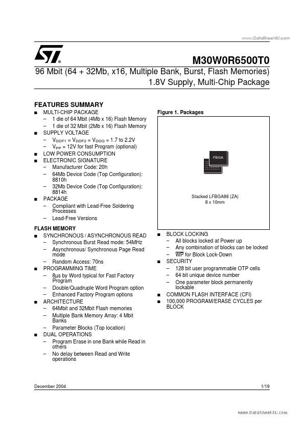
- Packages FBGA Stacked LFBGA88 (ZA) 8 x 10mm FLASH MEMORY
- SYNCHRONOUS / ASYNCHRONOUS READ – Synchronous Burst Read mode: 54MHz – Asynchronous/ Synchronous Page Read mode – Random Access: 70ns
- PROGRAMMING TIME – 8µs by Word typical for Fast Factory Program – Double/Quadruple Word Program option – Enhanced Factory Program options
- ARCHITECTURE – 64Mbit and 32Mbit Flash memories – Multiple Bank Memory Array: 4 Mbit Banks – Parameter Blocks (Top location)
- DUAL OPERATIONS – Program Erase in one Bank while Read in others – No delay between Read and Write operations