Datasheet4U Logo Datasheet4U.com

M50FW080 Datasheet 8 Mbit 1mb X8/ Uniform Block 3v Supply Firmware Hub Flash Memory

Manufacturer: STMicroelectronics

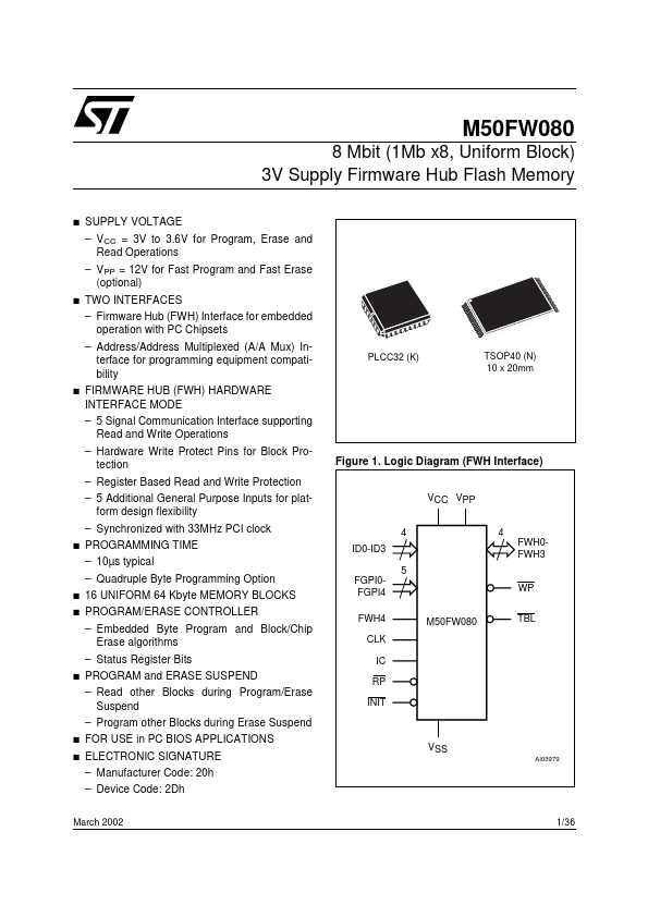
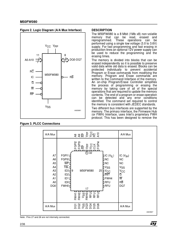
Overview: M50FW080 8 Mbit (1Mb x8, Uniform Block) 3V Supply Firmware Hub Flash Memory s SUPPLY VOLTAGE – VCC = 3V to 3.6V for Program, Erase and Read Operations – VPP = 12V for Fast Program and Fast Erase (optional) s TWO INTERFACES – Firmware Hub (FWH) Interface for embedded operation with PC Chipsets – Address/Address Multiplexed (A/A Mux) Interface for programming equipment patibility PLCC32 (K) TSOP40 (N) 10 x 20mm s FIRMWARE HUB (FWH) HARDWARE INTERFACE MODE – 5 Signal munication Interface supporting Read and Write Operations – Hardware Write Protect Pins for Block Protection – Register Based Read and Write Protection – 5 Additional General Purpose Inputs for platform design flexibility – Synchronized with 33MHz PCI clock 4 ID0-ID3 5 FGPI0FGPI4 FWH4 CLK IC RP INIT M50FW080 WP TBL VCC VPP 4 FWH0FWH3 Figure 1. Logic Diagram (FWH Interface) s PROGRAMMING TIME – 10µs typical – Quadruple Byte Programming Option s s 16 UNIFORM 64 Kbyte MEMORY BLOCKS PROGRAM/ERASE CONTROLLER – Embedded Byte Program and Block/Chip Erase algorithms – Status Register Bits s PROGRAM and ERASE SUSPEND – Read other Blocks during Program/Erase Suspend – Program other Blocks during Erase Suspend s s FOR USE in PC BIOS APPLICATIONS ELECTRONIC SIGNATURE – Manufacturer Code: 20h – Device Code: 2Dh VSS AI03979 March 2002 1/36 M50FW080 Figure 2.

General Description

The M50FW080 is a 8 Mbit (1Mb x8) non-volatile memory that can be read, erased and reprogrammed.

These operations can be performed using a single low voltage (3.0 to 3.6V) supply.

For fast programming and fast erasing in production lines an optional 12V power supply can be used to reduce the programming and the erasing times.

Key Features

  • e stress ratings only and operation of the device at these or any other conditions above those indicated in the.

M50FW080 Distributor