Datasheet4U Logo Datasheet4U.com

M50LPW116 - 16 Mbit 2Mb x8/ Boot Block 3V Supply Low Pin Count Flash Memory

Description

The M50LPW116 is a 16 Mbit (2Mb x8) nonvolatile memory that can be read, erased and reprogrammed.

These operations can be performed using a single low voltage (3.0 to 3.6V) supply.

Features

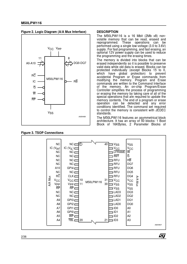
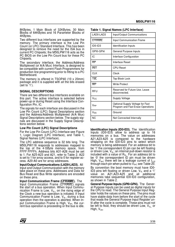
  • an asymmetrical block architecture. It has an array of 50 blocks: 1 Boot Block of 16KBytes, 2 Parameter Blocks of VCC VPP 11 A0-A10 8 DQ0-DQ7 RC IC G W RP M50LPW116 RB VSS AI05468 Figure 3. TSOP Connections NC IC (VIH) NC NC NC NC A10 NC RC VCC VPP RP NC NC A9 A8 A7 A6 A5 A4 NC IC (VIL) NC NC NC NC GPI4 NC CLK VCC VPP RP NC NC GPI3 GPI2 GPI1 GPI0 WP TBL 1 40 10 31 M50LPW116 11 30 20 21 VSS VCC LFRAME INIT RFU RFU RFU RFU RFU VCC VSS VSS LAD3 LAD2 LAD1 LAD0 ID0 ID1 ID2 ID3 VSS VCC W.

📥 Download Datasheet

Full PDF Text Transcription

Click to expand full text
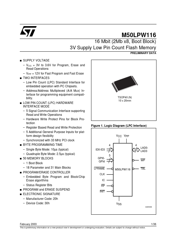
M50LPW116 16 Mbit (2Mb x8, Boot Block) 3V Supply Low Pin Count Flash Memory PRELIMINARY DATA s SUPPLY VOLTAGE – VCC = 3V to 3.6V for Program, Erase and Read Operations s – VPP = 12V for Fast Program and Fast Erase TWO INTERFACES – Low Pin Count (LPC) Standard Interface for embedded operation with PC Chipsets. – Address/Address Multiplexed (A/A Mux) Interface for programming equipment compatibility. s LOW PIN COUNT (LPC) HARDWARE INTERFACE MODE – 5 Signal Communication Interface supporting Read and Write Operations – Hardware Write Protect Pins for Block Protection – Register Based Read and Write Protection – 5 Additional General Purpose Inputs for platform design flexibility – Synchronized with 33 MHz PCI clock TSOP40 (N) 10 x 20mm Figure 1.
Published: |