Datasheet Details
| Part number | P6NC80 |
|---|---|
| Manufacturer | STMicroelectronics |
| File Size | 442.21 KB |
| Description | STP6NC80 |
| Datasheet | P6NC80_STMicroelectronics.pdf |
|
|
|
Overview: .. STP6NC80Z - STP6NC80ZFP STB6NC80Z - STB6NC80Z-1 N-CHANNEL 800V - 1.5Ω - 5.4A TO-220/FP/D²PAK/I²PAK Zener-Protected PowerMESH™III MOSFET TYPE STP6NC80Z/FP STB6NC80Z/-1 s s VDSS 800V 800V RDS(on) < 1.8 Ω < 1.8 Ω ID 5.4 A 5.4 A 1 3 s s s TYPICAL RDS(on) = 1.
| Part number | P6NC80 |
|---|---|
| Manufacturer | STMicroelectronics |
| File Size | 442.21 KB |
| Description | STP6NC80 |
| Datasheet | P6NC80_STMicroelectronics.pdf |
|
|
|
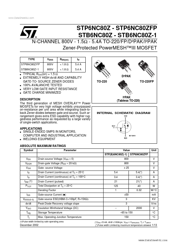
The third generation of MESH OVERLAY™ Power MOSFETs for very high voltage exhibits unsurpassed on-resistance per unit area while integrating back-toback Zener diodes between gate and source.
Such arrangement gives extra ESD capability with higher ruggedness performance as requested by a large variety of single-switch applications.
APPLICATIONS SINGLE-ENDED SMPS IN MONITORS, PUTER AND INDUSTRIAL APPLICATION s WELDING EQUIPMENT s I²PAK (Tabless TO-220) ABSOLUTE MAXIMUM RATINGS Symbol VDS VDGR VGS ID ID IDM (1) PTOT IGS VESD(G-S) dv/dt VISO Tstg Tj Parameter Drain-source Voltage (VGS = 0) Drain-gate Voltage (RGS = 20 kΩ) Gate- source Voltage Drain Current (continuous) at TC = 25°C Drain Current (continuous) at TC = 100°C Drain Current (pulsed) Total Dissipation at TC = 25°C Derating Factor Gate-source Current (q ) Gate source ESD(HBM-C=100pF, R=15KΩ) Peak Diode Recovery voltage slope Insulation Winthstand Voltage (DC) Storage Temperature Max.
| Part Number | Description |
|---|---|
| P6NC60 | STP6NC60 |
| P6N25 | STP6N25 |
| P6N60FI | STP6N60FI |
| P6NA60FI | STP6NA60FI |
| P6NB80FP | STP6NB80FP |
| P6NK90Z | N-CHANNEL MOSFET |