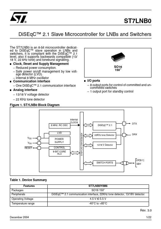
ST7LNB0
ST7LNB0 is Diseqc TM 2.1 Slave Microsontroller manufactured by STMicroelectronics.
Features
Packages Peripherals Operating Voltage Temperature range ST7LNB0Y0M6 SO16 150” Di SEq C™ 2.1 munication interface, 22KHz tone detector, 13/18V detector 4.5 V t0 5.5 V -40°C to +85°C
Rev. 3.0
December 2004 1/22
1 ST7LNB0 PIN DESCRIPTION
Figure 2 ST7LNB0 Pinout
VSS VDD RESET DRX OP5 OP6 OP7 OP8
1 2 3 4 5 6 7 8 16 15 14 13 12 11 10 9
NC NC DTX SBY OP1 OP2 OP3 OP4
The following table gives the pin functions Table 2. ST7LNB0 Pin Functions Pin Number 1 2 3 4 5 6 7 8 9 10 1) 11 12 13 14 15,16 Function Name Vss VDD RESET DRX OP5 OP6 OP7 OP8 OP4 OP3 OP2 OP1 SBY DTX Function Description
Ground Power Supply (+5 volts) Reset (active low) input Receive input output 5 (unmitted port) output 6 (unmitted port) output 7 (unmitted port) output 8 (unmitted port) output 4 (SO B/A) output 3 (SB/SA) output 2 (H/V) output 1 (Hi/Lo) STANDBY Di SEq C™ data transmit output Not used pins 2)
Notes: 1. During normal operation this pin must be pulled- up, internally or externally (external pull-up of 10k mandatory in noisy environment). This is to avoid entering ICC mode unexpectedly during a reset. In the application, even if the pin is configured as output, any reset will put it back in input pull-up 2. Unused pins 15 and 16 must be tied to ground.
2/22
2 ST7LNB0 IMPLEMENTATION
The following figure shows a typical application circuit for the ST7LNB0: Figure 3 ST7LNB0 typical application circuit
OPTIONAL
F-CONNECTOR
4.7K (4) ST7LNB0 2.2 n F 10n 330K 1 2 3 4 5 6 7 8 16 15 14 13 12 11 10 9 2N2222
SBY LNB / SWITCHER CONTROL (mitted SW)
100K
LNB / SWITCHER CONTROL (Unmitted SW)
Notes: 1.The divider chain connected to the DRX pin must have the following resistance values: 330KΩ and 100KΩ. 2.The reset circuitry linked to the RESET pin is optional, in fact the ST7LNB0 has an internal voltage level detector LVD which generates a static reset when the VDD supply is below a threshold voltage of 4.1 V. 3.The Di SEq C signalling must have a tone...