• Part: STB140NF55
  • Description: N-CHANNEL POWER MOSFET
  • Category: MOSFET
  • Manufacturer: STMicroelectronics
  • Size: 458.85 KB
Download STB140NF55 Datasheet PDF
STMicroelectronics
STB140NF55
STB140NF55 is N-CHANNEL POWER MOSFET manufactured by STMicroelectronics.
Features TYPE STB140NF55 STP140NF55 - 
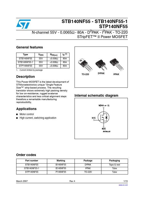
STB140NF55 STP140NF55 Figure 1:Package RDS(on) ID 80 A 80 A VDSS 55 V 55 V < 0.008 Ω < 0.008 Ω TYPICAL RDS(on) = 0.0065 Ω DESCRIPTION This Power Mosfet is the latest development of STMicroelectronis unique "Single Feature Size™" strip-based process. The resulting transistor shows extremely high packing density for low onresistance, rugged avalanche characteristics and less critical alignment steps therefore a remarkable manufacturing reproducibility. APPLICATIONS MOTOR CONTROL - HIGH CURRENT, SWITCHING APPLICATIONS - AUTOMOTIVE ENVIRONMENT - 3 1 3 1 2 D2PAK TO-263 (Suffix “T4”) TO-220 Figure 2: Internal Schematic Diagram .. Table 2: Order Codes Part Number STB140NF55T4 STP140NF55 MARKING B140NF55 P140NF55 PACKAGE D²PAK TO-220 PACKAGING TAPE & REEL TUBE Table 3:ABSOLUTE MAXIMUM RATINGS Symbol VDS VGS ID ID IDM(- ) Ptot dv/dt(1) EAS(2) Tstg Tj Parameter Drain-source Voltage (VGS = 0) Gate- source Voltage Drain Current (continuous) at TC = 25°C Drain Current (continuous) at TC = 100°C Drain Current (pulsed) Total Dissipation at TC = 25°C Derating Factor Peak Diode Recovery voltage slope Single Pulse Avalanche Energy Storage Temperature Operating Junction Temperature Value 55 ± 20 80 80 320 300 2 10 1.3 -55 to 175 (1) ISD ≤80A, di/dt ≤300A/µs, VDD ≤ V(BR)DSS, Tj ≤ TJMAX (2) Starting Tj = 25 o C, ID = 40A, VDD = 30V Unit V V A A A W W/°C V/ns m J °C (- ) Pulse width limited by safe operating area. (- - ) Current Limited by Package December 2004 Rev. 2 1/11 STB140NF55 STP140NF55 Table 4: THERMAL DATA Rthj-case Rthj-amb Tl Thermal Resistance Junction-case Thermal Resistance Junction-ambient Maximum Lead Temperature For Soldering Purpose Max Max 0.5 62.5 300 °C/W °C/W °C ELECTRICAL CHARACTERISTICS (Tcase = 25 °C unless otherwise specified) Table 5: OFF Symbol V(BR)DSS IDSS IGSS Parameter Drain-source Breakdown Voltage Zero Gate Voltage Drain Current (VGS = 0) Gate-body Leakage Current (VDS = 0) Test Conditions ID = 250...