STB25NM60N Overview
Key Specifications
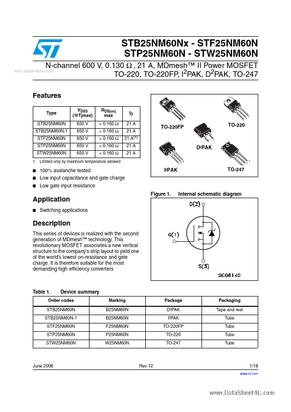
Package: D2PAK
Mount Type: Surface Mount
Pins: 3
Max Operating Temp: 150 °C
Description
This series of devices is realized with the second generation of MDmesh™ technology. This revolutionary MOSFET associates a new vertical structure to the company’s strip layout to yield one of the world’s lowest on-resistance and gate charge.
Key Features
- Limited only by maximum temperature allowed
- 100% avalanche tested
- Low input capacitance and gate charge
- Low gate input resistance