STB85NF55L
STB85NF55L is N-channel Power MOSFET manufactured by STMicroelectronics.
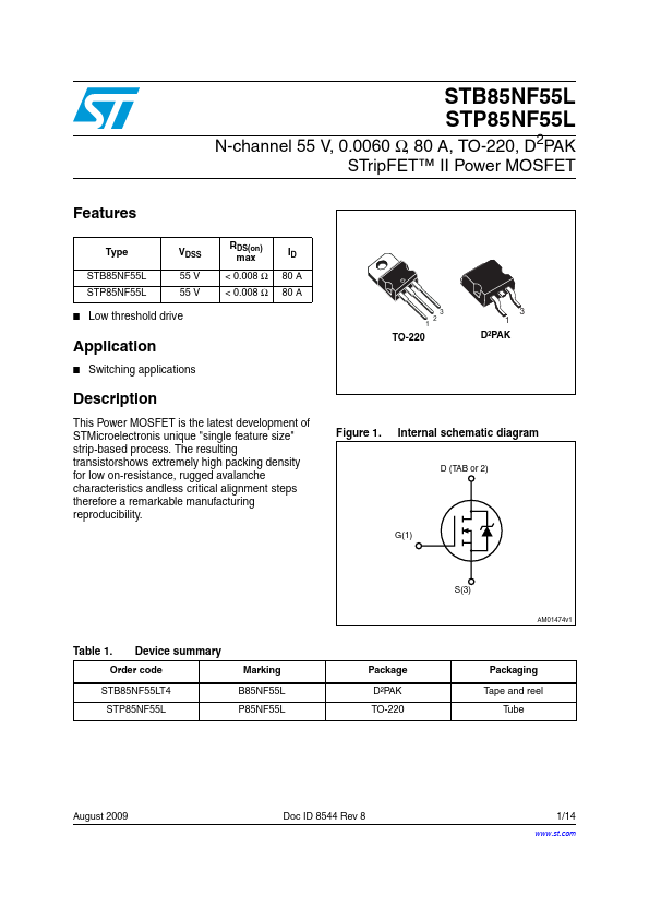
N This Power MOSFET is the latest development of STMicroelectronis unique "Single Feature Size™" strip-based process. The resulting transistor shows extremely high packing density for low onresistance, rugged avalanche characteristics and less critical alignment steps therefore a remarkable manufacturing reproducibility. APPLICATIONS s SOLENOID AND RELAY DRIVERS s MOTOR CONTROL, AUDIO AMPLIFIERS s DC-DC CONVERTERS s AUTOMOTIVE ENVIRONMENT
Ordering Information
SALES TYPE STP85NF55L STB85NF55L STB85NF55LT4 MARKING P85NF55L B85NF55L B85NF55L
D2PAK TO-263 (Suffix “T4”)
TO-220
ADD SUFFIX “T4” FOR ORDERING IN TAPE & REEL
INTERNAL SCHEMATIC DIAGRAM
PACKAGE TO-220 D2PAK D2PAK
PACKAGING TUBE TUBE TAPE & REEL
ABSOLUTE MAXIMUM RATINGS
Symbol VDS VDGR VGS ID(- ) ID IDM (-
- ) Ptot dv/dt (1) EAS (2) Tstg Tj Parameter Drain-source Voltage (VGS = 0) Drain-gate Voltage (RGS = 20 kΩ) Gate- source Voltage Drain Current (continuous) at TC = 25°C Drain Current (continuous) at TC = 100°C Drain Current (pulsed) Total Dissipation at TC = 25°C Derating Factor Peak Diode Recovery voltage slope Single Pulse Avalanche Energy Storage Temperature Max. Operating Junction Temperature Value 55 55 ± 15 80 80 320 300 2.0 10 980 -55 to 175 Unit V V V A A A W W/°C V/ns m J °C
(- ) Current Limited by Package. (-
- ) Pulse width limited by safe operating area. September 2002
1) ISD ≤80A, di/dt ≤300A/µs, VDD ≤ V (BR)DSS, Tj ≤ TJMAX (2) Starting T j = 25 o C, ID = 40A, VDD = 30V
1/10
STB85NF55L STP85NF55L
THERMAL DATA
Rthj-case Rthj-amb Tl Thermal Resistance Junction-case Thermal Resistance Junction-ambient Maximum Lead Temperature For Soldering Purpose Max Max 0.5 62.5 300 °C/W °C/W °C
ELECTRICAL CHARACTERISTICS (Tcase = 25 °C unless otherwise specified) OFF
Symbol V(BR)DSS IDSS IGSS Parameter Drain-source Breakdown Voltage Zero Gate Voltage Drain Current (VGS = 0) Gate-body Leakage Current (VDS = 0) Test Conditions ID = 250 µA, VGS = 0 VDS = Max Rating VDS = Max Rating TC = 125°C VGS = ± 15 V Min....