STP5NC50
STP5NC50 is N-Channel MOSFET manufactured by STMicroelectronics.
- STP5NC50FP STB5NC50
- STB5NC50-1
N-CHANNEL 500V
- 1.3Ω
- 5.5A TO-220/FP/D2PAK/I2PAK PowerMesh™ II MOSFET
TYPE STP5NC50 STP5NC50FP STB5NC50 STB5NC50-1 s s s s s
VDSS 500 500 500 500 V V V V
RDS(on) < 1.5Ω < 1.5Ω < 1.5Ω < 1.5Ω
ID 5.5A 5.5A 5.5A 5.5A
3 1
TYPICAL RDS(on) = 1.3Ω EXTREMELY HIGH dv/dt CAPABILITY 100% AVALANCHE TESTED NEW HIGH VOLTAGE BENCHMARK GATE CHARGE MINIMIZED
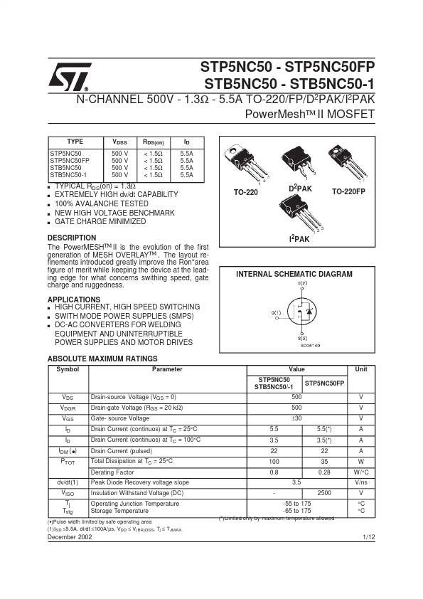
TO-220
D2PAK
TO-220FP
3 12
DESCRIPTION The PowerMESH™ II is the evolution of the first generation of MESH OVERLAY™ . The layout refinements introduced greatly improve the Ron- area figure of merit while keeping the device at the leading edge for what concerns swithing speed, gate charge and...