STW38NB20
STW38NB20 is N-Channel Power MOSFET manufactured by STMicroelectronics.
N-CHANNEL 200V
- 0.052 Ω
- 38A TO-247 Power MESH™ MOSFET
PRELIMINARY DATA
Table 1. General Features
Type
VDSS
RDS(on)
STW38NB20 200 V
< 0.065 Ω
ID 38 A
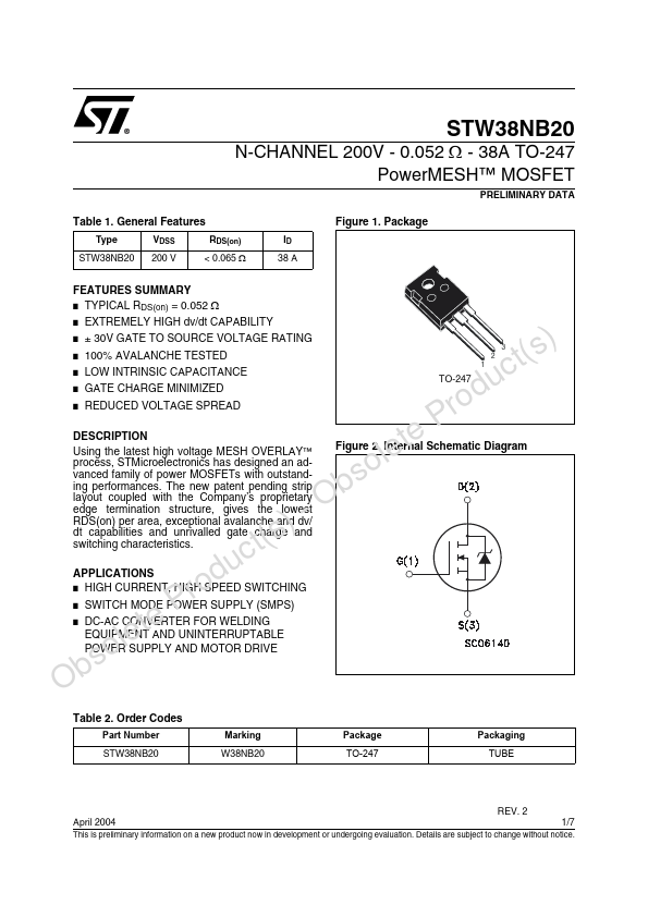
Figure 1. Package
Features
SUMMARY
- TYPICAL RDS(on) = 0.052 Ω
- EXTREMELY HIGH dv/dt CAPABILITY
- ± 30V GATE TO SOURCE VOLTAGE RATING t(s)
- 100% AVALANCHE TESTED c
- LOW INTRINSIC CAPACITANCE u
- GATE CHARGE MINIMIZED rod
- REDUCED VOLTAGE SPREAD
TO-247
3 2 1
P DESCRIPTION te Using the latest high voltage MESH OVERLAY™ le process, STMicroelectronics has designed an ado vanced family of power MOSFETs with outstands ing performances. The new patent pending strip b layout coupled with the pany’s proprietary O edge termination structure, gives the lowest
- RDS(on) per area, exceptional avalanche and dv/ ) dt capabilities and unrivalled gate charge and t(s switching characteristics.
Figure 2. Internal Schematic Diagram uc APPLICATIONS rod
- HIGH CURRENT, HIGH SPEED SWITCHING
- SWITCH MODE POWER SUPPLY (SMPS) te P
- DC-AC CONVERTER FOR WELDING EQUIPMENT AND UNINTERRUPTABLE
Obsole POWER SUPPLY AND MOTOR...