Datasheet4U Logo Datasheet4U.com

TDA7521 Datasheet Analog Front End

Manufacturer: STMicroelectronics

Overview: TDA7521 Analog Front End PRODUCT PREVIEW TDA7521 is a BiCMOS analog front end for CD applications. Four input signals (AC*, BD*, E* and F*), ing from the pick-up (whose laser diode is driven and controlled by the device itself), are preamplified by a programmable voltage-to-voltage or current-tovoltage stage, depending on the used pick-up. The output signals from the preamplifier stage (AC, BD, E, F and HF, a radio frequency signal obtained by bining the photo-detector outputs as A+B+C+D) are fed to an 8-bit HF ADC (for HF, which carries encoded audio data) and a 6-bit Servo ADC (for AC, BD, E and F, used for focusing, tracking the laser beam and controlling revolution speed). All these signals are digitized, multiplexed, synchronized with the external clock (768×Fs or 394×Fs, Fs=44.1KHz) and fed to the digital counterpart in one only digital stream (AC/HF/ BD/HF/E/HF/F/HF). Two stereo DACs convert the input bitstreams from TDA7522. TQFP44 (10 x 10 x 1.40 mm body) All the clock signals (for ADCs and DACs) are generated by a low-jitter PLL-based clock manager.

General Description

1.1 Clock source and generation The master clock to operate the device is 768 ×Fs (High Frequency mode, HFM) or 384 ×Fs (Low Frequency mode, LFM).

Fs=44.1KHz for CD applications.

In eith

Key Features

  • the functions ments an I2C-like protocol). 
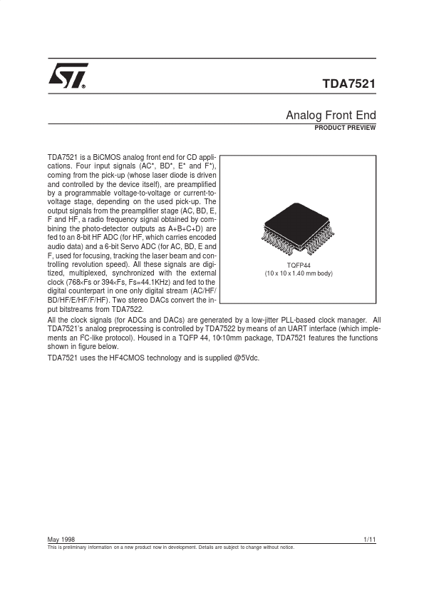
Housed in a TQFP 44, 10 shown in figure below. TDA7521 uses the HF4CMOS technology and is supplied @5Vdc. May 1998 This is preliminary information on a new product now in development. Details are subject to change without notice. 1/11 TDA7521 Figure 1. TDA7521 Block Diagram REXT REF OUT HF MON FILT REF IN PON REF Gen I/V CLOCK Mgr CKIN AC BD I/V RF ADC SYNC d0 d1 d2 d3 d4 d5 d6/OF d7/UF Output MUX E I/V F I/V Servo ADC Control I/F.

TDA7521 Distributor