36NM60N
Features
3 1 D2 PAK
Order code STB36NM60N
VDS @ TJmax
650 V
RDS(on) max.
ID PTOT
0.105 Ω 29 A 210 W
- Designed for automotive applications and AEC-Q101 qualified
- 100% avalanche tested
- Low input capacitance and gate charge
- Low gate input resistance
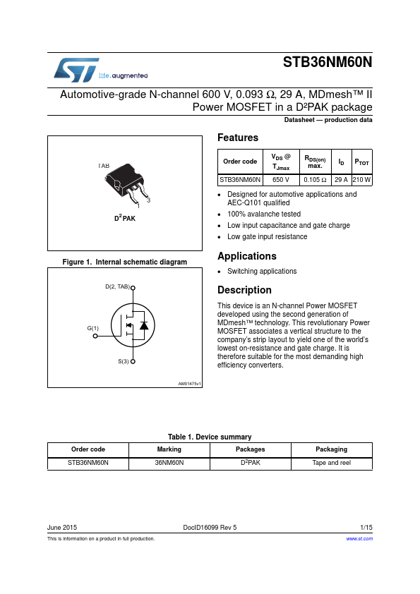
Figure 1. Internal schematic diagram
'7$%
- 6
Applications
- Switching applications
Description
This device is an N-channel Power MOSFET developed using the second generation of MDmesh™ technology. This revolutionary Power MOSFET associates a vertical structure to the pany’s strip layout to yield one of the world’s lowest on-resistance and gate charge. It is therefore suitable for the most demanding high efficiency converters.
$0Y
Order code STB36NM60N
Table 1. Device summary
Marking
Packages
D2PAK
Packaging Tape and reel
June 2015
This is information on a product in full production.
Doc ID16099 Rev 5
1/15
.st.
Contents
Contents
STB36NM60N
Electrical ratings
- - . ....