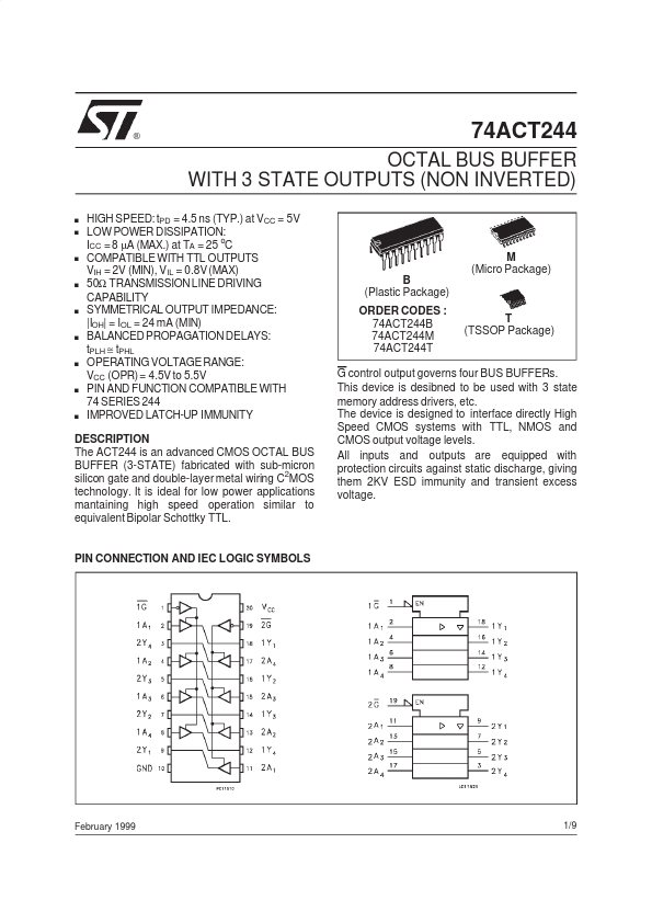
DESCRIPTION
G control output governs four BUS BUFFERs. This device is desibned to be used with 3 state memory address drivers, etc. The device is designed to interface directly High Speed CMOS systems with TTL, NMOS and CMOS output voltage levels. All inputs and outputs are equipped with protection circuits against static discharge, giving them 2KV ESD immunity and transient excess voltage. PIN CONNECTION AND IEC LOGIC SYMBOLS February 1999 1/9 74ACT244 INPUT AND OUTPUT EQUIVALENT CIRCUIT PIN DESCRIPTION
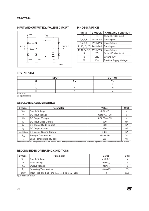
PIN No 1 2, 4,6, 8 9, 7,5, 3 11, 13, 15, 17 18, 16, 14, 12 19 10 20 SYMBOL 1G 1A1 to 1A4 2Y1 to 2Y4 2A1 to 2A4 1Y1 to 1Y4 2G GND VCC NAME AND FUNCT ION Output Enable Input Data Inputs Data Outputs Data Inputs Data Outputs Output Enabel Input Ground (0V) Positive Supply Voltage TRUTH TABLE INPUT G L L H X:”H” or ”L” Z: High impedance OUTPUT An L H X Yn L H Z ABSOLUTE MAXIMUM RATINGS
Symbol VCC VI VO IIK IOK IO ICC orIGND Tstg TL Supply Voltage DC Input Voltage DC Output Voltage DC Input... STMicroelectronics