Datasheet Details
| Part number | 74ACT299 |
|---|---|
| Manufacturer | STMicroelectronics |
| File Size | 102.18 KB |
| Description | 8 BIT PIPO SHIFT REGISTER |
| Datasheet | 74ACT299_STMicroelectronics.pdf |
|
|
|
Overview: ® 74ACT299 8 BIT PIPO SHIFT REGISTER WITH ASYNCHRONOUS CLEAR PRELIMINARY DATA s s s s s s s s s HIGH SPEED: fMAX = 170 MHz (TYP.) at VCC = 5V LOW POWER DISSIPATION: ICC = 8 µA (MAX.) at TA = 25 oC PATIBLE WITH TTL OUTPUTS VIH = 2V (MIN), VIL = 0.8V (MAX) 50Ω TRANSMISSION LINE DRIVING CAPABILITY SYMMETRICAL OUTPUT IMPEDANCE: |IOH| = IOL = 24 mA (MIN) BALANCED PROPAGATION DELAYS: tPLH ≅ tPHL OPERATING VOLTAGE RANGE: VCC (OPR) = 4.5V to 5.5V PIN AND FUNCTION PATIBLE WITH 74 SERIES 299 IMPROVED LATCH-UP IMMUNITY B M (Plastic Package) (Micro Package) ORDER CODES : 74ACT299B 74ACT299M These devices have four modes (HOLD, SHIFT LEFT, SHIFT RIGHT and LOAD DATA). Each mode is chosen by two function select inputs (S0, S1) as shown in the Truth Table. When one or both enable inputs, (G1, G2) are high, the eight input/output terminals are in the high-impedance state ; however sequential operation or clearing of the register is not affected. Clear function is synchronous to clock. The device is designed to interface directly High Speed CMOS systems with TTL, NMOS and CMOS output voltage levels. All inputs and outputs are equipped with protection circuits against static discharge, giving them 2KV ESD immunity and transient excess voltage.
| Part number | 74ACT299 |
|---|---|
| Manufacturer | STMicroelectronics |
| File Size | 102.18 KB |
| Description | 8 BIT PIPO SHIFT REGISTER |
| Datasheet | 74ACT299_STMicroelectronics.pdf |
|
|
|
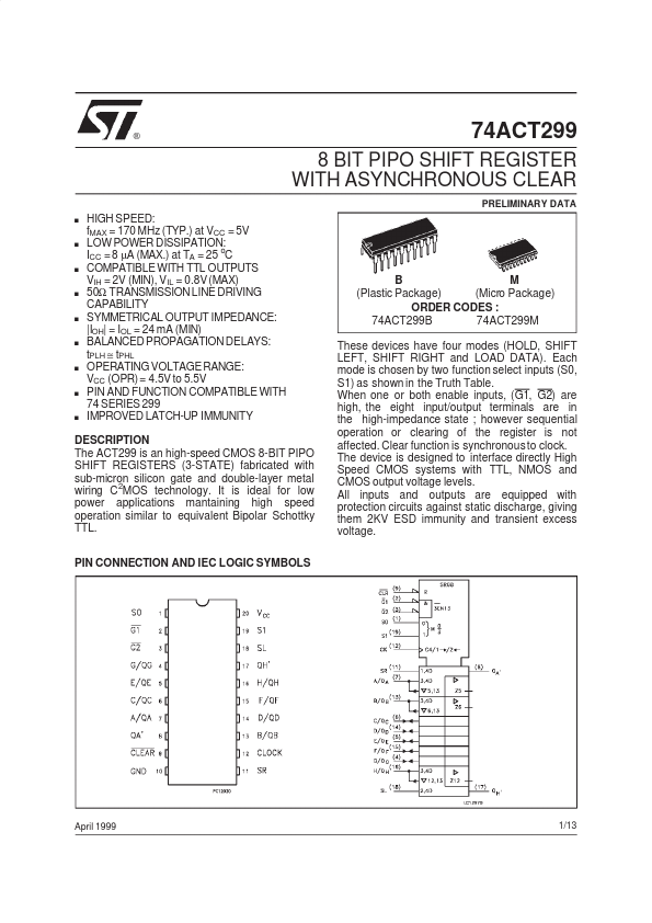
The ACT299 is an high-speed CMOS 8-BIT PIPO SHIFT REGISTERS (3-STATE) fabricated with sub-micron silicon gate and double-layer metal 2 wiring C MOS technology.
It is ideal for low power applications mantaining high speed operation similar to equivalent Bipolar Schottky TTL.
PIN CONNECTION AND IEC LOGIC SYMBOLS April 1999 1/13 74ACT299 INPUT AND OUTPUT EQUIVALENT CIRCUIT PIN DESCRIPTION PIN No 1, 19 2, 3 7, 13, 6, 14, 5, 15, 4, 16 8, 17 9 11 12 18 10 20 SYMBOL S0, S1 G1, G2 A/QA to H/QH QA’ to QH’ CLEAR SR CLOCK SL GND VCC NAME AND F UNCTION Mode Select Inputs 3 State Output Enable Inputs (Active LOW) Parallel Data Inputs or 3 State Parallel Outputs (Bus Driver) Serial Outputs (Standard Output) Asynchronous Mast
| Brand Logo | Part Number | Description | Other Manufacturers |
|---|---|---|---|
| 74ACT299 | 8-Input Universal Shift/Storage Register | Fairchild Semiconductor |
| Part Number | Description |
|---|---|
| 74ACT20 | DUAL 4-INPUT NAND GATE |
| 74ACT240 | OCTAL BUS BUFFER |
| 74ACT244 | OCTAL BUS BUFFER |
| 74ACT245 | OCTAL BUS TRANSCEIVER |
| 74ACT257 | QUAD 2 CHANNEL MULTIPLEXER |
| 74ACT273 | OCTAL D-TYPE FLIP-FLOP |
| 74ACT280 | 9 BIT PARITY GENERATOR/CHECKER |
| 74ACT00 | QUAD 2-INPUT NAND GATE |
| 74ACT02 | QUAD 2-INPUT NOR GATE |
| 74ACT04 | HEX INVERTER |