DESCRIPTION
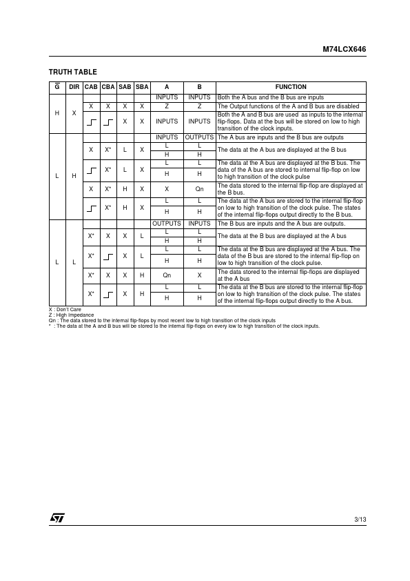
PIN CONNECTION AND IEC LOGIC SYMBOLS This device consists of bus transceiver circuits with 3 state, D-type flip-flops, and control circuitry arranged for multiplexed transmission of data directly from the input bus or from the internal registers. Data on the A or B bus will be clocked into register on the low to high transition of the appropriate clock pin (Clock AB or Clock BA). Enable (G) and direction (DIR) pins are provided to control the transceiver functions. In the transceiver mode, data present at the high-impedance port may be stored in either register or in both. The select controls (Select AB select BA) can multiplex stored and real time (transparent mode) data. The direction control determines which bus will receive data when enable G is active (low). In the isolation mode September 2001 1/13 M74LCX646 (enable G high), "A" data may be stored in one register and/or "B" data may be stored in the other register. When an output function is disabled, the input function is still enabled and may be used to store and transmit data. STMicroelectronics