Datasheet Details
| Part number | 74LVQ174 |
|---|---|
| Manufacturer | STMicroelectronics |
| File Size | 71.40 KB |
| Description | HEX D-TYPE FLIP FLOP |
| Datasheet | 74LVQ174_STMicroelectronics.pdf |
|
|
|
Overview: ® 74LVQ174 HEX D-TYPE FLIP FLOP WITH CLEAR s s s s s s s s s s s HIGH SPEED: fMAX = 150 MHz (TYP.) at VCC = 3.3V COMPATIBLE WITH TTL OUTPUTS LOW POWER DISSIPATION: ICC = 4 µA (MAX.) at TA = 25 oC LOW NOISE: VOLP = 0.3 V (TYP.) at VCC = 3.3V 75Ω TRANSMISSION LINE DRIVING CAPABILITY SYMMETRICAL OUTPUT IMPEDANCE: |IOH| = IOL = 12 mA (MIN) PCI BUS LEVELS GUARANTEED AT 24mA BALANCED PROPAGATION DELAYS: tPLH ≅ tPHL OPERATING VOLTAGE RANGE: VCC (OPR) = 2V to 3.6V (1.2V Data Retention) PIN AND FUNCTION COMPATIBLE WITH 74 SERIES 174 IMPROVED LATCH-UP IMMUNITY
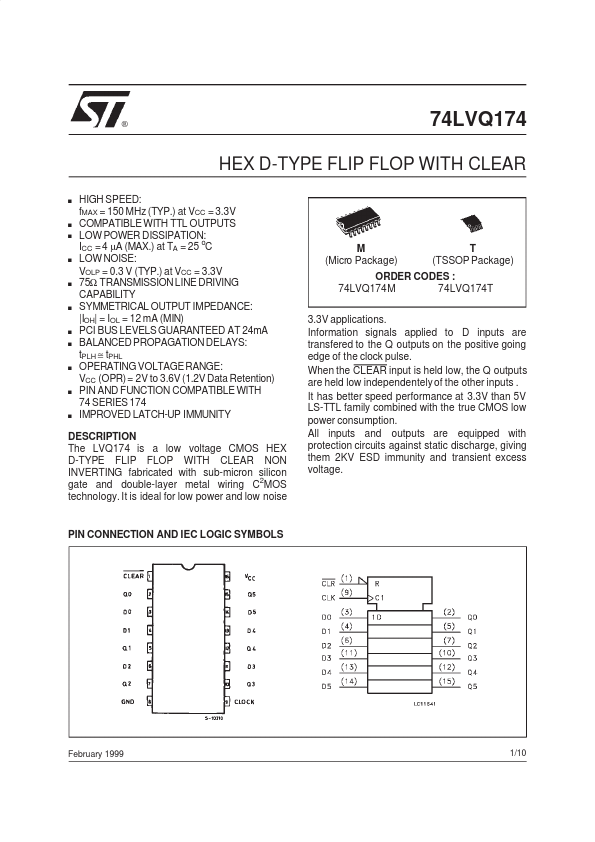
 M (Micro Package) T (TSSOP Package) ORDER CODES : 74LVQ174M 74LVQ174T 3.3V applications. Information signals applied to D inputs are transfered to the Q outputs on the positive going edge of the clock pulse. When the CLEAR input is held low, the Q outputs are held low independentely of the other inputs . It has better speed performance at 3.3V than 5V LS-TTL family combined with the true CMOS low power consumption. All inputs and outputs are equipped with protection circuits against static discharge, giving them 2KV ESD immunity and transient excess voltage.
| Part number | 74LVQ174 |
|---|---|
| Manufacturer | STMicroelectronics |
| File Size | 71.40 KB |
| Description | HEX D-TYPE FLIP FLOP |
| Datasheet | 74LVQ174_STMicroelectronics.pdf |
|
|
|
The LVQ174 is a low voltage CMOS HEX D-TYPE FLIP FLOP WITH CLEAR NON INVERTING fabricated with sub-micron silicon gate and double-layer metal wiring C2MOS technology.
It is ideal for low power and low noise PIN CONNECTION AND IEC LOGIC SYMBOLS February 1999 1/10 74LVQ174 INPUT AND OUTPUT EQUIVALENT CIRCUIT PIN DESCRIPTION PIN No 1 2, 5, 7, 10, 12, 15 3, 4, 6, 11, 13, 14 9 8 16 SYMBOL CLEAR Q0 to Q5 D0 to D5 CLOCK GND VCC NAME AND FUNCT ION Asyncronous Master Reset (Active LOW) Flip-Flop Outputs Data Inputs Clock Input (LOW-to-HIGH, Edge- Triggered) Ground (0V) Positive Supply Voltage TRUTH TABLE INPUTS CL EAR L H H H X:Don’t Care OUT PUT S CLO CK X Q L L H Qn F UNCTIO N CLEAR D X L H X NO CHANGE LOGIC DIAGRAM Thislogic diagram has notbe used to estimate propagation delays 2/10 74LVQ174 ABSOLUTE MAXIMUM RATINGS Symbol VCC VI VO
| Brand Logo | Part Number | Description | Manufacturer |
|---|---|---|---|
| 74LVQ174 | Low Voltage Hex D-Type Flip-Flop | Fairchild Semiconductor |
| Part Number | Description |
|---|---|
| 74LVQ125 | QUAD BUS BUFFERS 3-STATE |
| 74LVQ138 | 3 TO 8 LINE DECODER INVERTING |
| 74LVQ14 | HEX SCHMITT INVERTER |
| 74LVQ157 | LOW VOLTAGE QUAD 2 CHANNEL MULTIPLEXER |
| 74LVQ161 | SYNCHRONOUS PRESETTABLE 4-BIT COUNTER |
| 74LVQ163 | SYNCHRONOUS PRESETTABLE 4-BIT COUNTER |
| 74LVQ00 | QUAD 2-INPUT NAND GATE |
| 74LVQ02 | QUAD 2-INPUT NOR GATE |
| 74LVQ04 | HEX INVERTER |
| 74LVQ08 | QUAD 2-INPUT AND GATE |