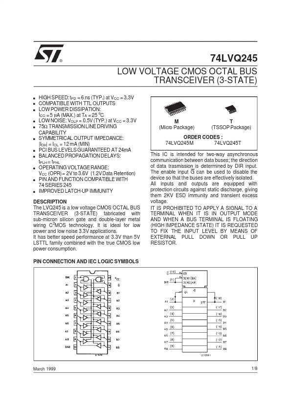
DESCRIPTION
It has better speed performance at 3.3V than 5V LSTTL family combined with the true CMOS low power consumption. PIN CONNECTION AND IEC LOGIC SYMBOLS March 1999 1/8 74LVQ245 INPUT EQUIVALENT CIRCUIT PIN DESCRIPTION
PIN No 1 2, 3, 4, 5, 6, 7, 8, 9 18, 17, 16, 15, 14, 13, 12, 11 19 10 20 SYMBOL DIR A1 to A8 B1 to B8 NAME AND FUNCT ION Directional Control Data Inputs/Outputs Data Inputs/Outputs G GND VCC Output Enable Input Ground (0V) Positive Supply Voltage TRUTH TABLE INPUT G L L H X:”H” or ”L” Z: High impedance F UNCTION DIR L H X A BUS OUTPUT INPUT Z B BUS INPUT OUTPUT Z OUT PUT A=B B=A Z ABSOLUTE MAXIMUM RATINGS
Symbol VCC VI VI/O IIK IOK IO Tstg TL Supply Voltage DC Input Voltage (DIR, G) DC Bus I/O Voltage DC Input Diode Current DC Output Diode Current DC Output Current Storage Temperature Lead Temperature (10 sec) Parameter Value -0.5 to +7 -0.5 to VCC + 0.5 -0.5 to VCC + 0.5 ± 20 ± 20 ± 50 ± 400 -65 to +150 300 Unit V V V mA mA mA mA o o ICC or IGND DC VCC or Ground Current C C ABSOLUTE MAXIMUM RATINGS
are those values beyond which damage to the device may occur. STMicroelectronics