DESCRIPTION
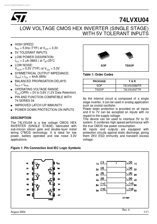
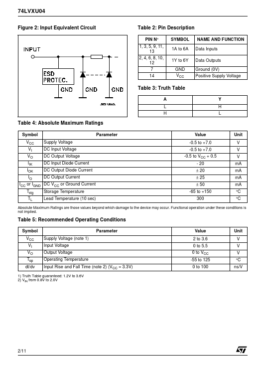
Figure 1: Pin Connection And IEC Logic Symbols As the internal circuit is composed of a single stage inverter, it can be used in analog application such as crystal oscillator. Power down protection is provided on all inputs and 0 to 7V can be accepted on inputs with no regard to the supply voltage. It combines high speed performance with the true CMOS low power consumption. All inputs and outputs are equipped with protection circuits against static discharge, giving them 2KV ESD immunity and transient excess voltage. August 2004 Rev. 4 1/11 74LVXU04 Figure 2: Input Equivalent Circuit Table 2: Pin DESCRIPTION
PIN N° 1, 3, 5, 9, 11, 13 2, 4, 6, 8, 10, 12 7 14 SYMBOL 1A to 6A 1Y to 6Y GND VCC NAME AND FUNCTION Data Inputs Data Outputs Ground (0V) Positive Supply Voltage Table 3: Truth Table A L H Y H L Table 4: ABSOLUTE MAXIMUM RATINGS
Symbol VCC VI VO IIK IOK IO Tstg TL Supply Voltage DC Input Voltage DC Output Voltage DC Input Diode Current DC Output Diode Current DC Output... STMicroelectronics