STMicroelectronics 74LX1G125
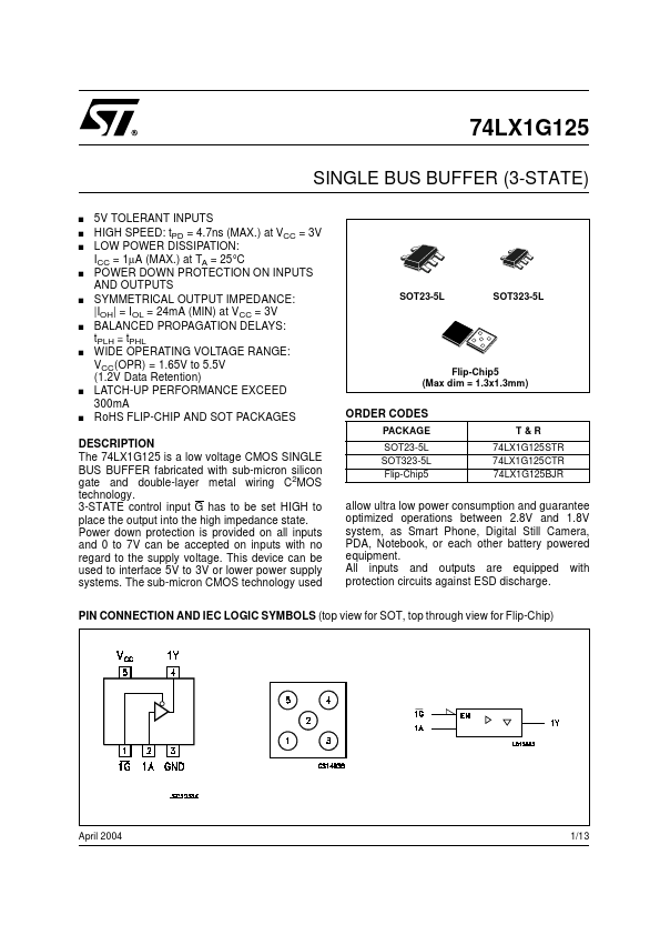
The 74LX1G125 is a low voltage CMOS SINGLE BUS BUFFER fabricated with sub-micron silicon gate and double-layer metal wiring C2MOS technology. This device can be used to interface 5V to 3V or lower power supply systems. The sub-micron CMOS technology used allow ultra low power consumption and guarantee optimized operations between 2.8V and 1.8V system, as Smart Phone, Digital Still Camera, PDA, Notebook, or each other battery powered equipment.| Part No. | 74LX1G125 |
|---|---|
| Datasheet | 74LX1G125 Download |
| Manufacturer |  STMicroelectronics |
| Description | SINGLE BUS BUFFER |
| Buy | Stock & Price |
DESCRIPTION
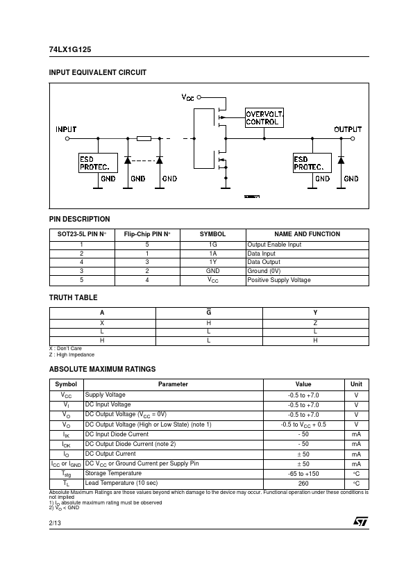
3-STATE control input G has to be set HIGH to place the output into the high impedance state. Power down protection is provided on all inputs and 0 to 7V can be accepted on inputs with no regard to the supply voltage. All inputs and outputs are equipped with protection circuits against ESD discharge. PIN CONNECTION AND IEC LOGIC SYMBOLS (top view for SOT, top through view for Flip-Chip) April 2004 1/13 74LX1G125 INPUT EQUIVALENT CIRCUIT PINDESCRIPTION
SOT23-5L PIN N° 1 2 4 3 5 Flip-Chip PIN N° 5 1 3 2 4 SYMBOL 1G 1A 1Y GND VCC NAME AND FUNCTION Output Enable Input Data Input Data Output Ground (0V) Positive Supply Voltage TRUTH TABLE A X L H X : Don’t Care Z : High Impedance G H L L Y Z L HABSOLUTE MAXIMUM RATINGS
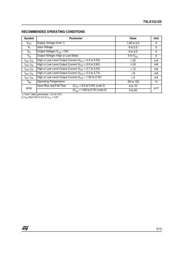
Symbol VCC VI VO VO IIK IOK IO Supply Voltage DC Input Voltage DC Output Voltage (VCC = 0V) DC Output Voltage (High or Low State) (note 1) DC Input Diode Current DC Output Diode Current (note 2) DC Output Current Parameter Value -0.5 to +7.0 -0.5 to +7.0 -0.5 to...