DESCRIPTION
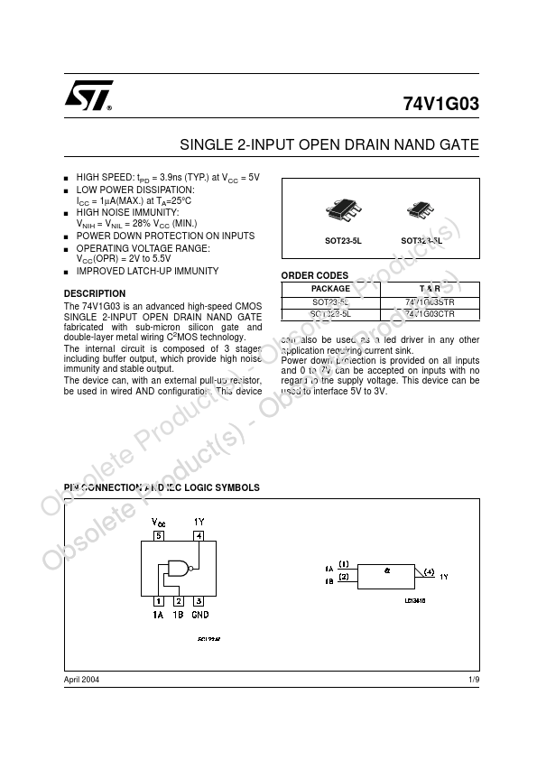
) leThe device can, with an external pull-up resistor, t(s obe used in wired AND configuration. Power down protection is provided on all inputs and 0 to 7V can be accepted on inputs with no regard to the supply voltage. This device can be used to interface 5V to 3V. OObbssoolleettee PPrroodduucct(s) - ObsPIN CONNECTION AND IEC LOGIC SYMBOLS April 2004 1/9 74V1G03 INPUT EQUIVALENT CIRCUIT PIN DESCRIPTION
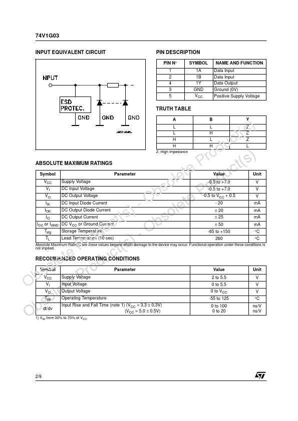
PIN N° 1 2 4 3 5 SYMBOL 1A 1B 1Y GND VCC NAME AND FUNCTION Data Input Data Input Data Output Ground (0V) Positive Supply Voltage TRUTH TABLE A L t(s)L H cH duZ: High Impedance B L H L H Y Z Z Z L Pro t(s)ABSOLUTE MAXIMUM RATINGS
te cSymbol Parameter Value Unit le duVCC Supply Voltage -0.5 to +7.0 V so roVI DC Input Voltage -0.5 to +7.0 V b PVO DC Output Voltage -0.5 to VCC + 0.5 V - O teIIK DC Input Diode Current - 20 mA ) leIOK DC Output Diode Current ± 20 mA t(s oIO DC Output Current ± 25 mA c bsICC or IGND DC VCC or Ground Current ± 50 mA u OTstg Storage Temperature -65 to +150 °C d -TL Lead Temperature (10 sec) 260 °C ro )ABSOLUTE MAXIMUM RATINGS
are those values beyond which damage to the device may occur. STMicroelectronics