DESCRIPTION
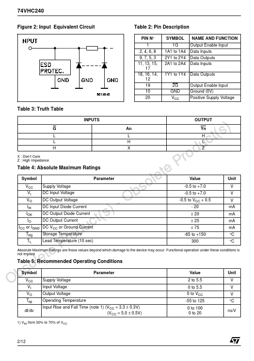
PIN N° 1 2, 4, 6, 8 9, 7, 5, 3 11, 13, 15, 17 18, 16, 14, 12 19 10 20 SYMBOL NAME AND FUNCTION 1G 1A1 to 1A4 2Y1 to 2Y4 2A1 to 2A4 Output Enable Input Data Inputs Data Outputs Data Inputs 1Y1 to 1Y4 Data Outputs 2G GND VCC Output Enable Input Ground (0V) Positive Supply Voltage Table 3: Truth Table INPUTS )G t(sL L ucH rodX : Don‘t Care Z : High Impedance PTable 4: ABSOLUTE MAXIMUM RATINGS
An L H X OUTPUT Yn H L Z leteSymbol Parameter oVCC Supply Voltage bsVI DC Input Voltage OVO DC Output Voltage -IIK DC Input Diode Current )IOK DC Output Diode Current t(sIO DC Output Current cICC or IGND DC VCC or Ground Current duTstg Storage Temperature roTL Lead Temperature (10 sec) Value -0.5 to +7.0 -0.5 to +7.0 -0.5 to VCC + 0.5 - 20 ± 20 ± 25 ± 75 -65 to +150 300 Unit V V V mA mA mA mA °C °C PAbsolute MAXIMUM RATINGS
are those values beyond which damage to the device may occur. Functional operation under these conditions is tenot implied leTable 5: Recommended Operating Conditions... STMicroelectronics