DESCRIPTION
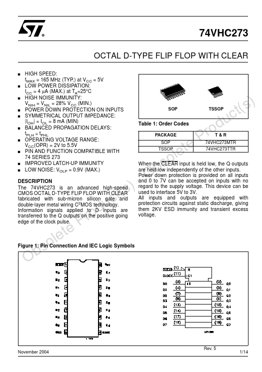
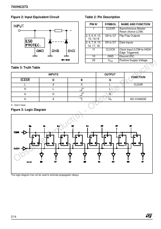
) du Information signals applied to D inputs are ro transferred to the Q outputs on the positive going edge of the clock pulse. SOP TSSOP Table 1: Order Codes PACKAGE SOP TSSOP T&R 74VHC273MTR 74VHC273TTR When the CLEAR input is held low, the Q outputs are held low independently of the other inputs. Power down protection is provided on all inputs and 0 to 7V can be accepted on inputs with no regard to the supply voltage. This device can be used to interface 5V to 3V. All inputs and outputs are equipped with protection circuits against static discharge, giving them 2KV ESD immunity and transient excess voltage. Obsolete P Figure 1: Pin Connection And IEC Logic Symbols November 2004 Rev. 5 1/14 74VHC273 Figure 2: Input Equivalent Circuit Table 2: Pin DESCRIPTION
PIN N° SYMBOL NAME AND FUNCTION 1 CLEAR Asynchronous Master Reset (Active LOW) 2, 5, 6, 9, 12, Q0 to Q7 Flip-Flop Outputs 15, 16,19 3, 4, 7, 8, 13, D0 to D7 Data Inputs 14, 17, 18 11 CLOCK Clock Input (LOW-to-HIGH Edg... STMicroelectronics