APPLICATIONS
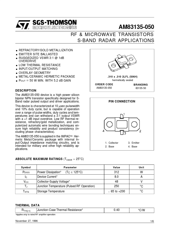
. . . . . . . . REFRACTORY/GOLD METALLIZATION EMITTER SITE BALLASTED RUGGEDIZED VSWR 3:1 @ 1dB OVERDRIVE LOW THERMAL RESISTANCE INPUT/OUTPUT MATCHING OVERLAY GEOMETRY METAL/CERAMIC HERMETIC PACKAGE POUT = 50 W MIN. WITH 5.2 dB GAIN .310 x .310 2LF L (S064) hermetically sealed O RDER CODE AM83135-050 BRANDING 83135-50 DESCRIPTION
Low RF thermal resistance, refractory/gold metallization, and computerized automatic wire bonding techniques ensure high reliability and product consistency (including phase characteristics). ABSOLUTE MAXIMUM RATINGS
(T case = 25° C) Symbol Parameter PIN CONNECTION 1. Collector 2. Base 3. Emitter 4. Base Value Un it PDISS IC VCC TJ TSTG Power Dissipation* Device Current* (TC ≤ 125 °C) 312 8.0 48 250 − 65 to +200 W A V °C °C Collector-Supply Voltage* Junction Temperature (Pulsed RF Operation) Storage Temperature THERMAL DATA RTH(j-c) Junction-Case Thermal Resistance* 0.40 °C/W *Applies only to rated RF amplifier operation November 27, 1996 1/6 AM83135-050 ELECTRICAL SPECIFICATIONS
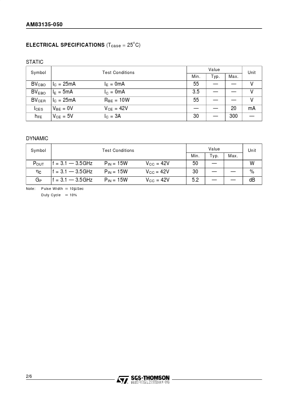
(T case = 25° C) STATIC Symbol Test Conditions Value Min. STMicroelectronics