DESCRIPTION
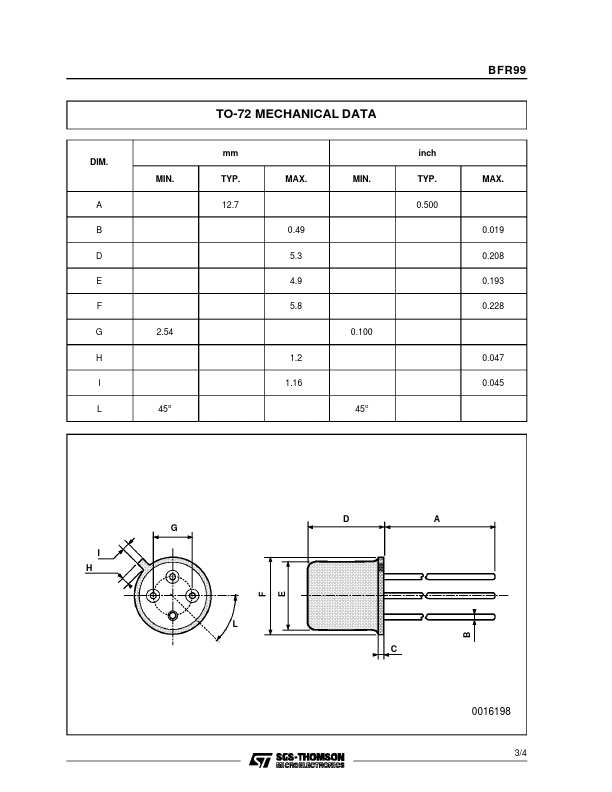
TO-72 INTERNAL SCHEMATIC DIAGRAM ABSOLUTE MAXIMUM RATINGS
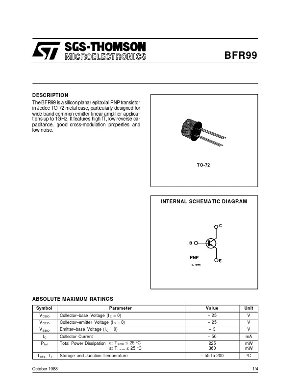
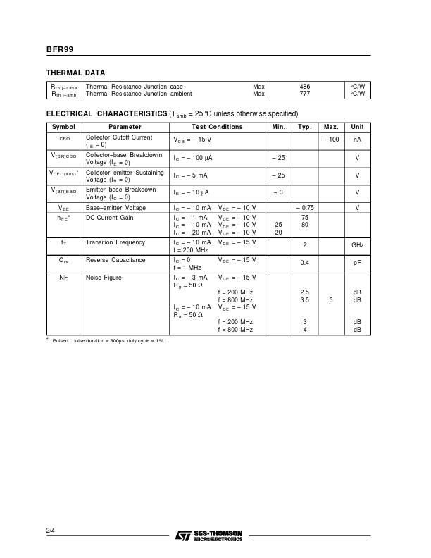
Symbol VCBO VCEO VEBO IC Pto t Tstg, Tj Parameter Collector–base Voltage (I E = 0) Collector–emitter Voltage (IB = 0) Emitter–base Voltage (I C = 0) Collector Current Total Power Dissipation at T amb ≤ 25 °C at T cas e ≤ 25 °C Storage and Junction Temperature October 1988 V al ue – 25 – 25 –3 – 50 225 360 – 55 to 200 Unit V V V mA mW mW °C 1/4 BFR99 THERMAL DATA R th j– c as e Thermal Resistance Junction–case Rth j– amb Thermal Resistance Junction–ambient Max 486 Max 777 °C/W °C/W ELECTRICAL CHARACTERISTICS
(T amb = 25 °C unless otherwise specified) Symbol ICBO V(B R)CBO VCE O(sus)* V(B R)E BO VBE hFE* Parameter Collector Cutoff Current (IE = 0) Collector–base Breakdowm Voltage (IE = 0) Collector–emitter Sustaining Voltage (IB = 0) Emitter–base Breakdown Voltage (IC = 0) Base–emitter Voltage DC Current Gain fT Transition Frequency C re Reverse Capacitance NF Noise Figure * Pulsed : pulse duration = 300µs, duty cycle = 1%. STMicroelectronics