BFW43
BFW43 is HIGH VOLTAGE AMPLIFIER manufactured by STMicroelectronics.
DESCRIPTION
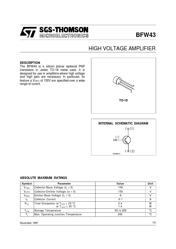
The BFW43 is a silicon planar epitaxial PNP transistors in Jedec TO-18 metal case. It is designed for use in amplifiers where high voltage and high gain are necessary. In particular, its feature a VCEO of 150V are specified over a wide range of curent.
TO-18
INTERNAL SCHEMATIC DIAGRAM
ABSOLUTE MAXIMUM RATINGS
Symbol V CBO V CEO V EBO IC P t ot T stg Tj Parameter Collector-Base Voltage (IE = 0) Collector-Emitter Voltage (I B = 0) Emitter-Base Voltage (I C = 0) Collector Current Total Dissipation at T amb ≤ 25 C at T case ≤ 25 o C St orage Temperature Max. Operating Junction Temperature o
Value -150 -150 -6 -0.1 0.4 1.4 -55 to 200 200
Unit V V V A W W o o
C C 1/5
November 1997
THERMAL DATA
R t hj-ca se R t hj- amb Thermal Resistance Junction-Case Thermal Resistance Junction-Ambient Max Max 125 438 o o
C/W C/W
ELECTRICAL CHARACTERISTICS (Tcase = 25 o C unless otherwise specified)
Symb ol I CBO Parameter Collector Cut-off Current (IE = 0) Test Cond ition s V CE = -100 V V CE = -100 V I C = -10 µ A T a mb = 125 o C -150 Min. Typ . -0.2 -0.03 Max. -10 -10 Un it n A µA V
V ( BR)CBO ∗ Collector-Base Breakdown Voltage (I E = 0) V ( BR)CEO ∗ Collector-Emitter Breakdown Voltage (I B = 0) V (BR)EBO ∗ Emitter-Base Breakdown Voltage (I C = 0) V CE(sat )∗ V BE(s at)∗ h FE∗ Collector-Emitter Saturation Voltage Base-Emitter Saturation Voltage DC Current G ain
I C = -2 m A
-150
I E = -10 µ A
-6
I C = -10 m A I C = -10 m A I C = -1 m A I C = -10 m A I C = -10 µ A T amb = -55 o C V CE = -10 V I C = -1 m A I C = -10 m A IE = 0 IE = 0
IB = -1 m A IB = -1 m A VCE = -10 V V CE = -10 V V CE = -10 V f = 20 MHz 40 40
-0.1 -0.74 85 100 30 50 60 f = 1MHz 20 5
-0.5 -0.9
V V f T
Transition F requency
MHz MHz 25 7 p F p F
C EBO C CBO
Emitter Base Capacitance Collector Base Capacitance
V EB = -0.5 V V CB = -5 V f = 1MHz
∗ Pulsed: Pulse duration = 300 µs, duty cycle ≤ 1 %
DC Current Gain.
Collector-emitter Saturation Voltage.
2/5
Base-emitter Saturation...