STMicroelectronics BUL3N7
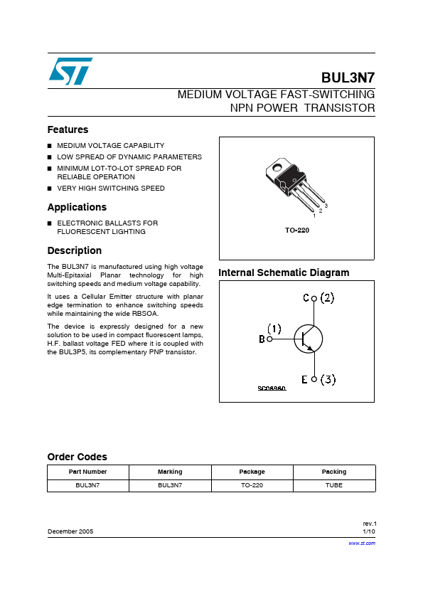
The BUL3N7 is manufactured using high voltage Multi-Epitaxial Planar technology for high switching speeds and medium voltage capability. It uses a Cellular Emitter structure with planar edge termination to enhance switching speeds while maintaining the wide RBSOA. The device is expressly designed for a new solution to be used in compact fluorescent lamps, H.F.| Part No. | BUL3N7 |
|---|---|
| Datasheet | BUL3N7 Download |
| Manufacturer |  STMicroelectronics |
| Description | MEDIUM VOLTAGE FAST-SWITCHING NPN POWER TRANSISTOR |
| Buy | Stock & Price |
FEATURES
●●
●
● MEDIUM VOLTAGE CAPABILITY LOW SPREAD OF DYNAMIC PARAMETERS MINIMUM LOT-TO-LOT SPREAD FOR RELIABLE OPERATION VERY HIGH SWITCHING SPEED 2 3
APPLICATIONS
● 1 ELECTRONIC BALLASTS FOR FLUORESCENT LIGHTING TO-220DESCRIPTION
ballast voltage FED where it is coupled with the BUL3P5, its complementary PNP transistor. Internal Schematic Diagram Order Codes Part Number BUL3N7 Marking BUL3N7 Package TO-220 Packing TUBE December 2005 rev.1 1/10 10 1ABSOLUTE MAXIMUM RATINGS
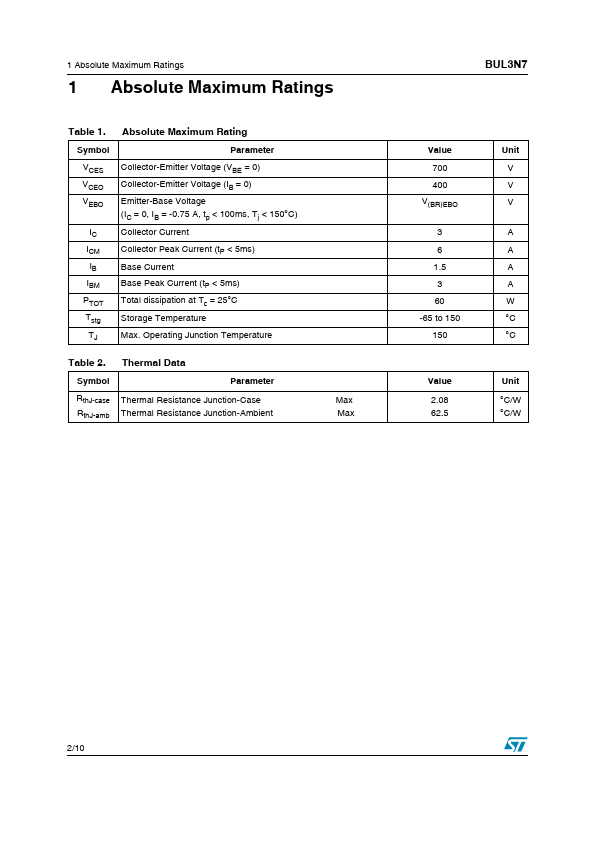
BUL3N7 1 Table 1. Symbol VCES VCEO VEBO IC ICM IB IBM PTOT Tstg TJABSOLUTE MAXIMUM RATINGS
Absolute Maximum Rating Parameter Collector-Emitter Voltage (VBE = 0) Collector-Emitter Voltage (IB = 0) Emitter-Base Voltage (IC = 0, IB = -0.75 A, tp < 100ms, Tj < 150°C) Collector Current Collector Peak Current (tP < 5ms) Base Current Base Peak Current (tP < 5ms) Total dissipation at Tc = 25°C Storage Temperature Max. Operating Junction Temperature Value 700 400 V(BR)EBO 3 6 1.5 3 60 -65 to 150 150 Unit V V V A A A A W °C °C Table 2.