STMicroelectronics DA108S
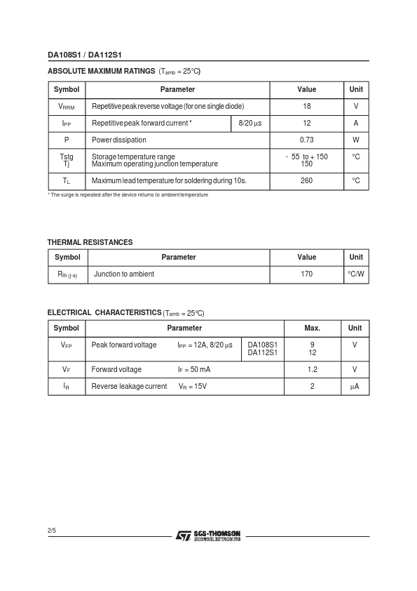
The surge is repeated after the device returns to ambient temperature THERMAL RESISTANCES Symbol Rth (j-a) Junction to ambient Parameter Value 170 Unit °C/W ELECTRICAL CHARACTERISTICS (Tamb = 25°C) Symbol VFP VF IR Peak forward voltage Forward voltage Reverse leakage current Parameter IPP = 12A, 8/20 µs IF = 50 mA VR = 15V DA108S1 DA112S1 Max.| Part No. | DA108S |
|---|---|
| Datasheet | DA108S Download |
| Manufacturer |  STMicroelectronics |
| Description | DIODE ARRAY |
| Buy | Stock & Price |
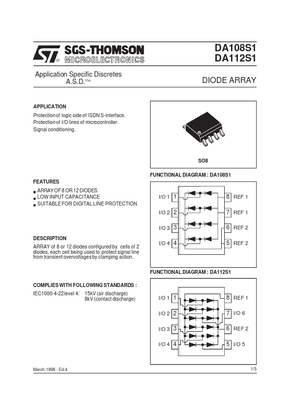
FEATURES
ARRAY OF 8 OR 12 DIODES LOW INPUT CAPACITANCE SUITABLE FOR DIGITAL LINE PROTECTION I/O 1 1 I/O 2 2 I/O 3 3 8 REF 1 7 REF 1 6 REF 2 5 REF 2DESCRIPTION
ARRAY of 8 or 12 diodes configured by cells of 2 diodes, each cell being used to protect signal line from transient overvoltages by clamping action. I/O 4 4 FUNCTIONAL DIAGRAM : DA112S1 COMPLIES WITH FOLLOWING STANDARDS : IEC1000-4-22level 4: 15kV (air discharge) 8kV (contact discharge) I/O 1 1 I/O 2 2 I/O 3 3 I/O 4 4 8 REF 1 7 I/O 6 6 REF 2 5 I/O 5 March 1998 - Ed:4 1/5 DA108S1 / DA112S1ABSOLUTE MAXIMUM RATINGS
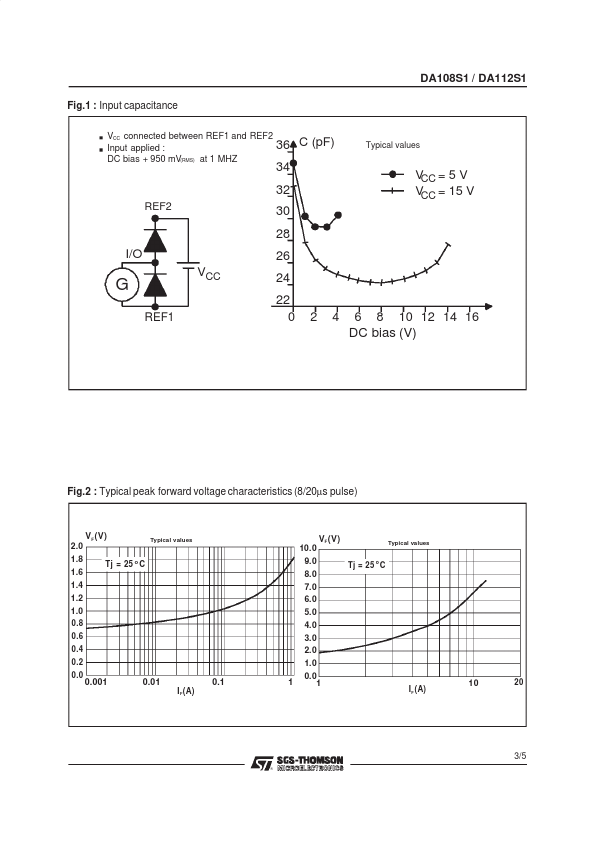
(Tamb = 25°C) Symbol VRRM IPP P Tstg Tj TL Parameter Repetitivepeak reverse voltage(forone single diode) Repetitive peak forward current * Power dissipation Storage temperature range Maximum operating junction temperature Maximum lead temperature for soldering during 10s. 8/20 µs Value 18 12 0.73 - 55 to + 150 150 260 Unit V A W °C °C * 9 12 1.2 2 Unit V V µA 2/5 ® DA108S1 / DA112S1 Fig.1 : Input capacitance VCC connect...