STMicroelectronics ETC5067
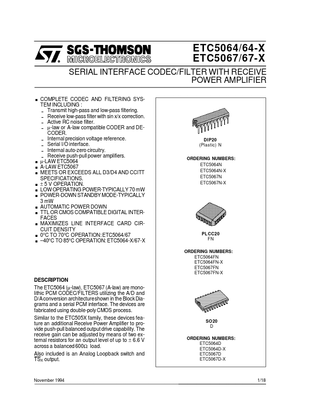
The ETC5064 (µ-law), ETC5067 (A-law) are monolithic PCM CODEC/FILTERS utilizing the A/D and D/A conversion architectureshown in the Block Diagrams and a serial PCM interface. The devices are fabricated using double-poly CMOS process. The receive gain can be adjusted by means of two external resistors for an output level of up to ± 6.6 V across a balanced 600Ω load.| Part No. | ETC5067 |
|---|---|
| Datasheet | ETC5067 Download |
| Manufacturer |  STMicroelectronics |
| Description | POWER AMPLIFIER SERIAL INTERFACE CODEC/FILTERWITH RECEIVE |
| Buy | Stock & Price |
DESCRIPTION
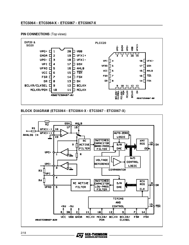
Similar to the ETC505X family, these devices feature an additional Receive Power Amplifier to provide push-pull balanced output drive capability. Also included is an Analog Loopback switch and TSX output. SO 20 D ORDERING NUMBERS: ETC5064D ETC5064D-X ETC5067D ETC5067D-X November 1994 1/18 ETC5064 - ETC5064-X - ETC5067 - ETC5067-X PIN CONNECTIONS (Top views) DIP20 & SO20 PLCC20 BLOCK DIAGRAM (ETC5064 - ETC5064-X - ETC5067 - ETC5067-X) 2/18 ETC5064 - ETC5064-X - ETC5067 - ETC5067-X PINDESCRIPTION
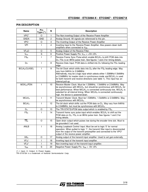
Name VPO + Pi n Type (*) O GND O I O S I I I N 1 2 3 4 5 6 7 8 9DESCRIPTION
The Non-inverting Output of the Receive Power Amplifier Analog Ground. All signals are referenced to this pin. The Inverting Output of the Receive Power Amplifier Inverting Input to the Receive Power Amplifier. Also powers down both amplifiers when connected to VBB. Analog Output of the Receive Filter. Positive Power Supply Pin. VCC = +5V ±5% Receive Frame Sync Pulse which enable BCLKR to shift PCM data into D R.