DESCRIPTION
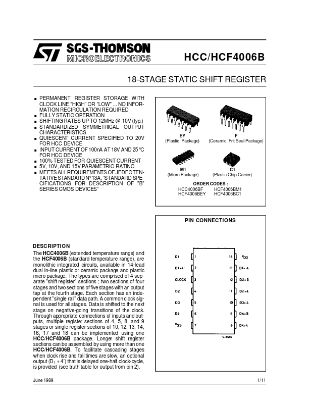
OF ”B” SERIES CMOS DEVICES” EY (Plastic Package) F (Ceramic Frit Seal Package) M1 (Micro Package) C1 (Plastic Chip Carrier) ORDER CODES : HCC4006BF HCF4006BM1 HCF4006BEY HCF4006BC1 PIN CONNECTIONS DESCRIPTION
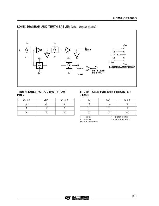
A common clock signal is used for all stages. Data is shifted to the next stage on negative-going transitions of the clock. Through appropriate connections of inputs and outputs, multiple register sections of 4, 5, 8, and 9 stages or single register sections of 10, 12, 13, 14, 16, 17 and 18 can be implemented using one HCC/HCF4006B package. Longer shift register sections can be assembled by using more than one HCC/HCF4006B. To facilitate cascading stages when clock rise and fall times are slow, an optional output (D1 + 4’) that is delayed one-half clock-cycle, is provided (see truth table for output from pin 2). June 1989 1/11 HCC/HCF4006B FUNCTIONAL DIAGRAM ABSOLUTE MAXIMUM RATINGS
Symbol V DD* Vi II Pt ot Parameter Supply Voltage : HCC Types HC F Types Input Voltage... STMicroelectronics