APPLICATIONS
FULLY STATIC OPERATION...DC TO 10MHz (typ.) @ VDD = 10V BUFFERED INPUTS AND OUTPUTS SINGLE-PHASE CLOCKING STANDARDIZED SYMMETRICAL OUTPUT CHARACTERISTICS QUIESCENT CURRENT SPECIFIED TO 20V FOR HCC DEVICE 5V, 10V, AND 15V PARAMETRIC RATING INPUT CURRENT OF 100nA AT 18V AND 25°C FOR HCC DEVICE 100% TESTED FOR QUIESCENT CURRENT MEETS ALL REQUIREMENTS OF JEDEC TENTATIVE STANDARD N° 13A, ”STANDARD SPECIFICATIONS FOR DESCRIPTION
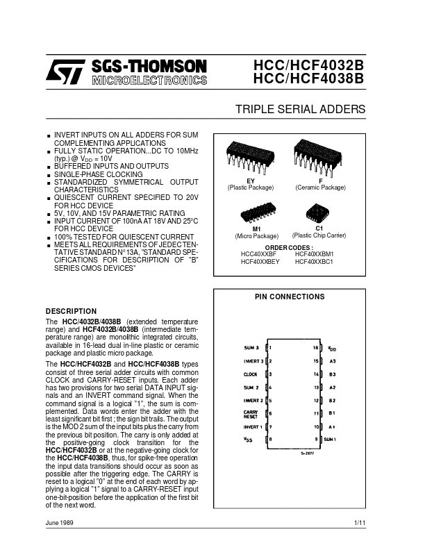
OF ”B” SERIES CMOS DEVICES” EY (Plastic Package) F (Ceramic Package) M1 (Micro Package) C1 (Plastic Chip Carrier) ORDER CODES : HCC40XXBF HCF40XXBM1 HCF40XXBEY HCF40XXBC1 PIN CONNECTIONS DESCRIPTION
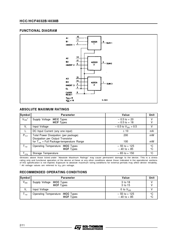
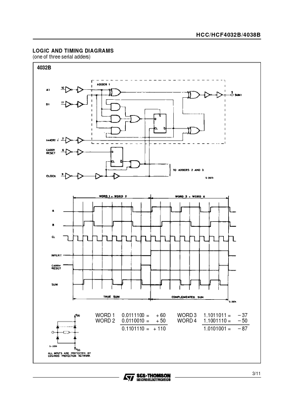
When the command signal is a logical ”1”, the sum is complemented. Data words enter the adder with the least significant bit first ; the sign bit trails. The output is the MOD 2 sum of the input bits plus the carry from the previous bit position. The carry is only added at the positive-going clock transition for the HCC/HCF4032B or at the negative-going clock for the HCC/HCF4038B, thus, for spike-free operation the input data transitions should occur as soon as possible after the triggering edge. STMicroelectronics