DESCRIPTION
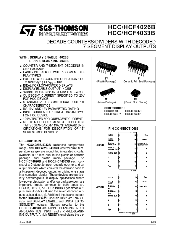
OF ”B” SERIES CMOS DEVICES” EY (Plastic Package) F (Ceramic Frit Seal Package) M1 (Micro Package) C1 (Plastic Chip Carrier) ORDER CODES : HCC40XXBF HCF40XXBM1 HCF40XXBEY HCF40XXBC1 PIN CONNECTIONS DESCRIPTION
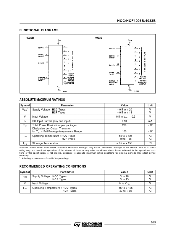
Inputs common to both types are CLOCK, RESET, & CLOCK INHIBIT ; common outputs are CARRY OUT and the seven decoded outputs (a, b, c, d, e, f, g). Additional inputs and outputs for the HCC/HCF4026B include DISPLAY ENABLE input and DISPLAY ENABLE and UNGATED ”CSEGMENT” outputs. Signals peculiar to the HCC/HCF4033B are RIPPLE-BLANKING INPUT AND LAMP TEST INPUT and a RIPPLE-BLANKING OUTPUT. A high RESET signal clears the deJune 1989 4026B 4033B 1/15 HCC/HCF4026B/4033B cade counter to its zero count. The counter is advanced one count at the positive clock signal transition if the CLOCK INHIBIT signal is low. Counter advancement via the clock line is inhibited when the CLOCK INHIBIT signal is high. Antilock gating is provided on the JOHNSON counter, thus assuring proper counting sequence. STMicroelectronics