DESCRIPTION
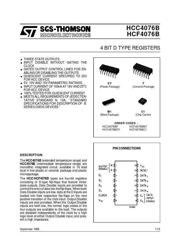
OF B SERIES CMOS DEVICES ” EY (Plastic Package) F (Ceramic Package) M1 (Micro Package) C1 (Chip Carrier) ORDER CODES : HCC4076BF HCF4076BM1 HCF4076BEY HCF4076BC1 PIN CONNECTIONS DESCRIPTION
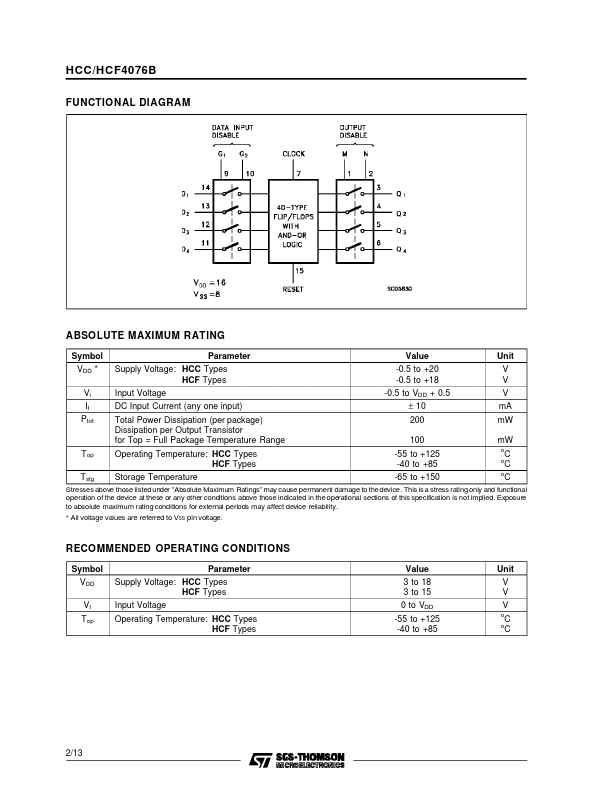
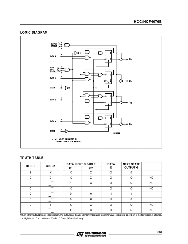
Data Disable inputs are provided to control the entry of data into theflip-flops. Output Disable inputs are also provided. When the Output Disable inputs are both low, the normal logic states of the four outputs are available to the load. The outputs are disabled independently of the clock by a high logic level at either Output Disable input, and present a high impedance. September 1988 1/13 HCC/HCF4076B FUNCTIONAL DIAGRAM ABSOLUTE MAXIMUM RATING Symbol VDD * Vi II Ptot Parameter Supply Voltage: HCC Types HCF Types Input Voltage DC Input Current (any one input) Total Power Dissipation (per package) Dissipation per Output Transistor for Top = Full Package Temperature Range Operating Temperature: HCC Types HCF Types Storage Temperature Value -0.5 to +20 -0.5 to +18 -0.5 to VDD + 0.5 ± 10 2... STMicroelectronics