STMicroelectronics HCC4085B
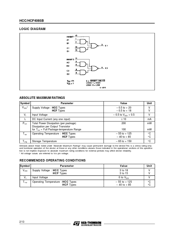
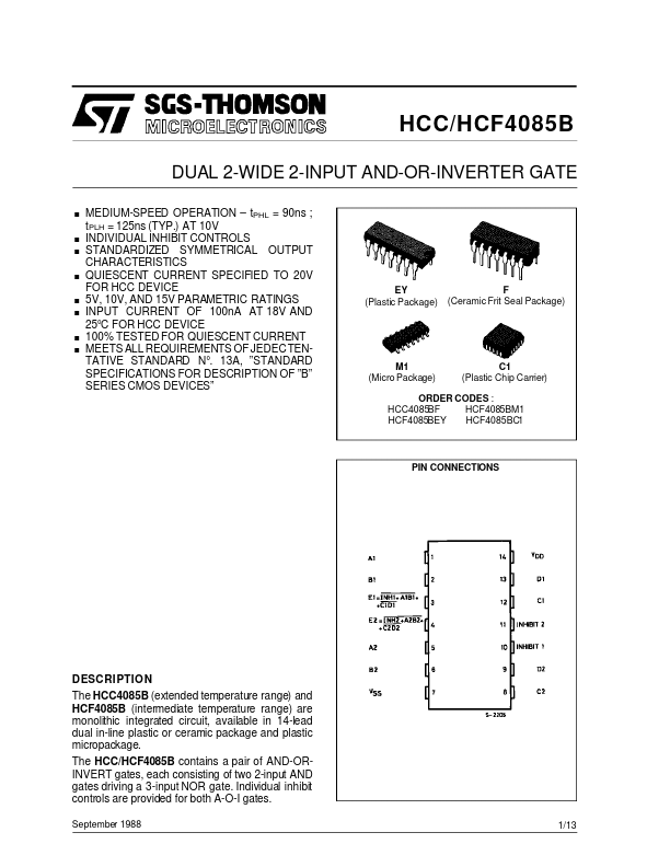
The HCC4085B (extended temperature range) and HCF4085B (intermediate temperature range) are monolithic integrated circuit, available in 14-lead dual in-line plastic or ceramic package and plastic micropackage. The HCC/HCF4085B contains a pair of AND-ORINVERT gates, each consisting of two 2-input AND gates driving a 3-input NOR gate.| Part No. | HCC4085B |
|---|---|
| Datasheet | HCC4085B Download |
| Manufacturer |  STMicroelectronics |
| Description | DUAL 2-WIDE 2-INPUT AND-OR-INVERTER GATE |
| Buy | Stock & Price |
DESCRIPTION
OF ”B” SERIES CMOS DEVICES” EY (Plastic Package) F (Ceramic Frit Seal Package) M1 (Micro Package) C1 (Plastic Chip Carrier) ORDER CODES : HCC4085BF HCF4085BM1 HCF4085BEY HCF4085BC1 PIN CONNECTIONSDESCRIPTION
Individual inhibit controls are provided for both A-O-I gates. September 1988 1/13 HCC/HCF4085B LOGIC DIAGRAMABSOLUTE MAXIMUM RATINGS
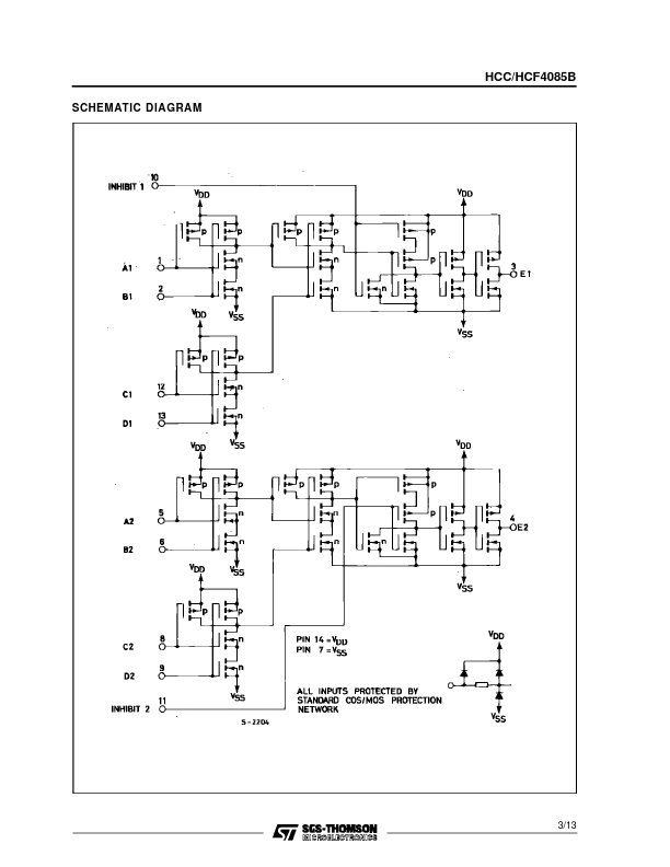
Symbol V DD * Vi II P tot Parameter Supply Voltage : HCC Types HCF Types Input Voltage DC Input Current (any one input) Total Power Dissipation (per package) Dissipation per Output Transistor for Top = Full Package-temperature Range Operating Temperature : HCC Types HCF Types Storage Temperature Value – 0.5 to + 20 – 0.5 to + 18 – 0.5 to V DD + 0.5 ± 10 200 100 – 55 to + 125 – 40 to + 85 – 65 to + 150 Unit V V V mA mW mW °C °C °C T op T s tg Stresses above those listed under ”ABSOLUTE MAXIMUM RATINGS
” may cause permanent damage to the device.This is a stress rating only and functional operation of the device at those or any other conditions aboves those indicated in the operational sections of this specification is not implied.