DESCRIPTION
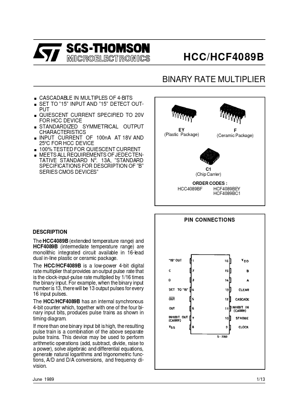
OF ”B” SERIES CMOS DEVICES” EY (Plastic Package) F (Ceramic Package) C1 (Chip Carrier) ORDER CODES : HCC4089BF HCF4089BEY HCF4089BC1 PIN CONNECTIONS DESCRIPTION
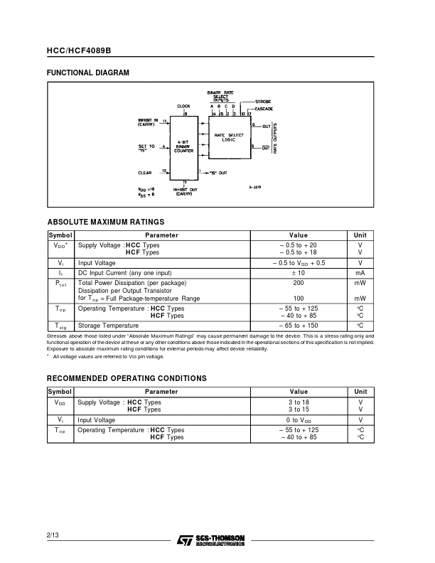
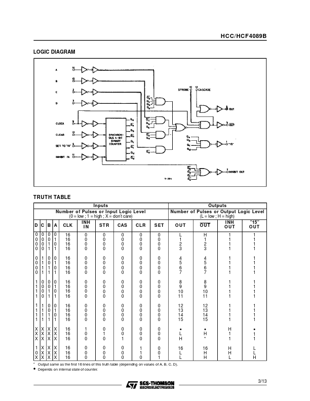
The HCC/HCF4089B has an internal synchronous 4-bit counter which, together with one of the four binary input bits, produces pulse trains as shown in timing diagram. If more than one binary input bit is high, the resulting pulse train is a combination of the above separate pulse trains. This device may be used to perform arithmetic operations (add, subtract, divide, raise to a power), solve algebraic and differential equations, generate natural logarithms and trigonometric functions, A/D and D/A conversions, and frequency division. June 1989 1/13 HCC/HCF4089B FUNCTIONAL DIAGRAM ABSOLUTE MAXIMUM RATINGS
Symbol V DD * Vi II Pt o t Parameter Supply Voltage : H CC Types H C F Types Input Voltage DC Input Current (any one input) Total Power Dissipation (per package) Dissipation per Output Transistor for T o p = Full Packa... STMicroelectronics