DESCRIPTION
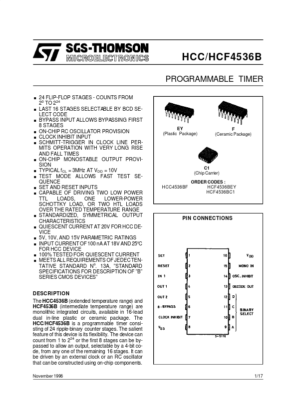
OF ”B” SERIES CMOS DEVICES” EY (Plastic Package) F (Ceramic Package) C1 (Chip Carrier) HCC4536BF ORDER CODES : HCF4536BEY HCF4536BC1 PIN CONNECTIONS DESCRIPTION
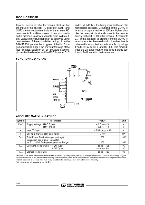
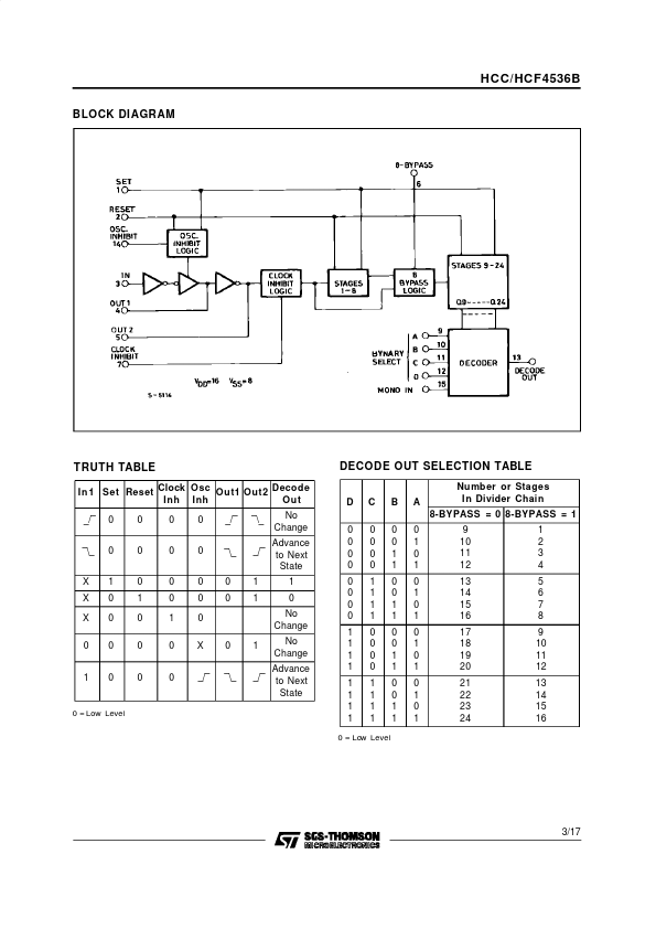
The device can count from 1 to 224 or the first 8 stages can be bypassed to allow an output, selectable by a 4-bit code, from any one of the remaining 16 stages. It can be driven by an external clock or an RC oscillator that can be constructed using on-chip components. November 1996 1/17 HCC/HCF4536B Input IN1 serves as either the external clock input or the input to the on-chip RC oscillator. OUT1 and OUT2 are connection terminals for the external RC components. In addition, an on-chip monostable circuit is provided to allow a variable pulse width output. Various timing functions can be achieved using combinations of these capabilities. A logic 1 on the 8-BYPASS input enables a bypass of the first 8 stages and makes stage 9 the first counter stage of the last 16 stages. Selection of 1 of 16 outputs is accomplished by the decoder and the BCD inputs A, B, C FUNCTIONAL DIAGRAM and D. STMicroelectronics